Hi team,
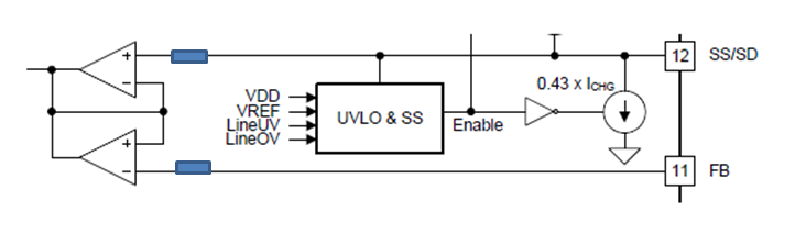
As the datasheet shown, the amplifier output will be the lower voltage of VFB and Vss. How to understand the this amplifier configuration work principle?
Thanks

Hi team,
As the datasheet shown, the amplifier output will be the lower voltage of VFB and Vss. How to understand the this amplifier configuration work principle?
Thanks