This thread has been locked.

If you have a related question, please click the "Ask a related question" button in the top right corner. The newly created question will be automatically linked to this question.

TPS63802: Can't make this part work.

Part Number: TPS63802
Other Parts Discussed in Thread: BQ24073

Hello,

I've designed a board that uses a TPS63802.

Its input is the output of a BQ24073, which, as I'm sure you already know, is a battery management IC able to automatically adjust the power path depending if the battery is charging or not.

From the voltage output of the BQ24073, which may be 3.7V or 4.8V from USB, I need to get 5V. I've chosen the TPS63802 because the max input would be too close from the desired output for a boost regulator to work.

Thing is, I've already burnt 6 pieces of it. No matter what I do, the moment I pull the EN pin high, the IC gets instantly hot and the output fixes at 0.4V. I've checked solders, the rest of the circuit, etc. and even done several tests on a naked board where I only soldered this IC an related passives, all with the same results.

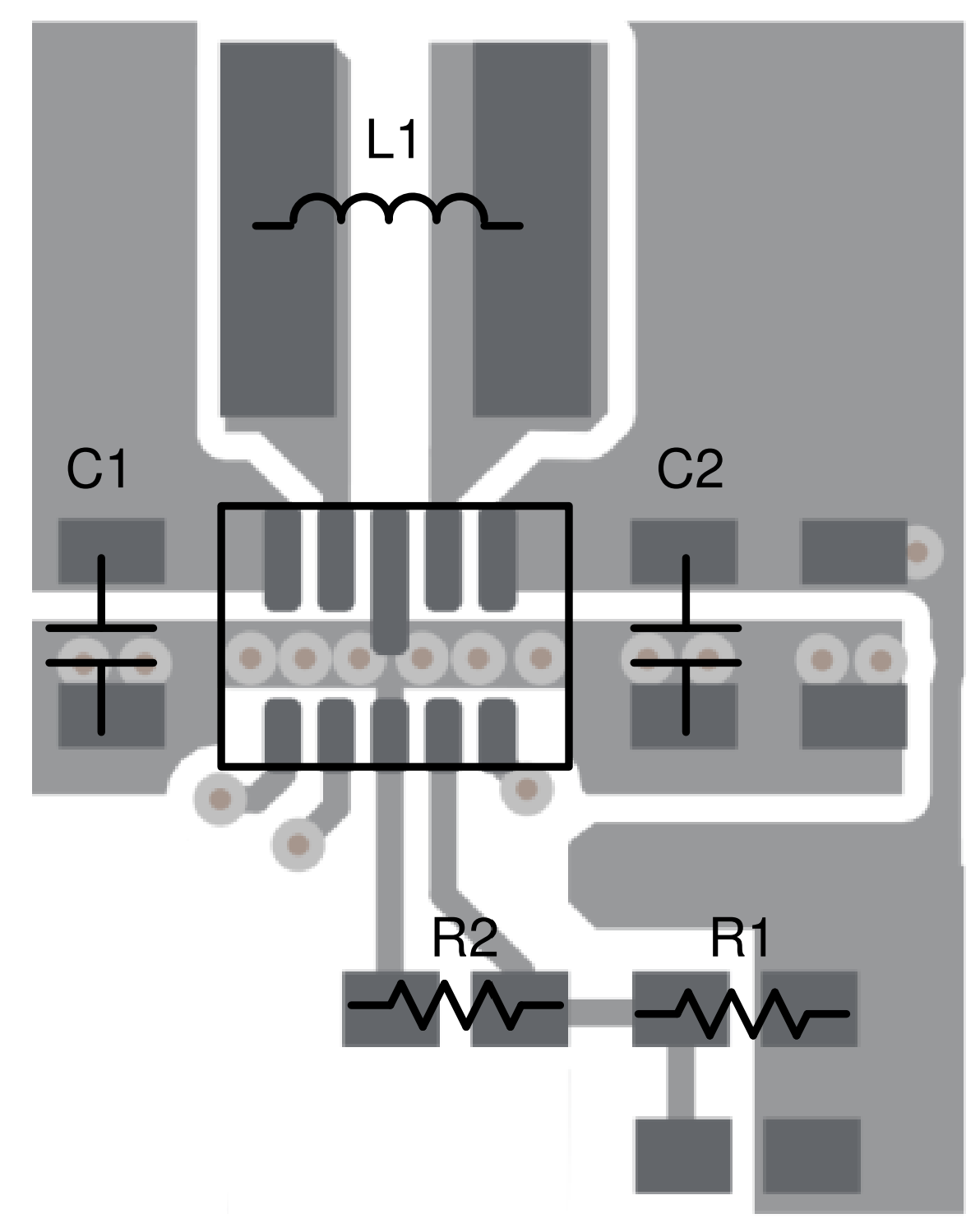
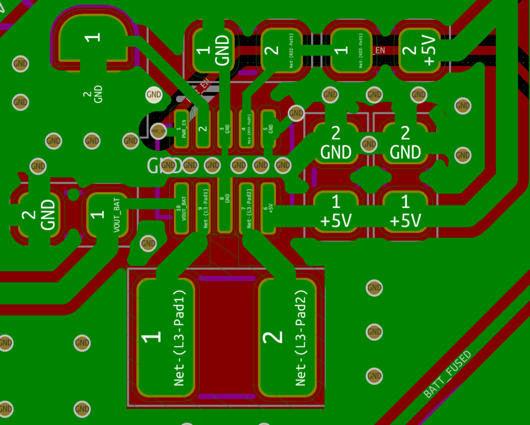
This is the layout (please note it's the bottom layer of the PCB):

Note VOUT_BAT net is the output of the BQ24073.

Feedback resistor values are 806k and 91k respectively, as the datasheet states. Inductor is LQH32PNR47NNCL from Murata, I believe it meets the requirements. Input and output caps are CC0603MRX6S5BB226 from Yageo, 22uF.

Can anyone lend a hand? I'm really desperate about this :(

Best regards,

Enrique

  • Hi Enrique,

    Thank you for reaching out.

    Just to double check, this is the bottom layer seen from top? 

    I see two potential causes for the device to fail:

    1. The minimum recommended output capacitance for Vout = 5 V is 7 μF. For CC0603MRX6S5BB226, the effective capacitance at 5 V is only 6.6 μF, which is below the minimum recommended. For Vout = 5 V we recommend using 2x 22 μF. Otherwise the device can become unstable, leading to oscillations and failure, especially when coupled with the second point below. 
    2. The PCB layout, or the GND routing to be precise, needs significant improvements. Please see the recommended layout in the datasheet and try to follow it as close as possible. In short:
      1. First place the input and output capacitors as close as possible to the device.
      2. Connect the GND ends of the input/output capacitors, GND and AGND pins directly, under the device.
      3. Adding multiple vias is recommended to improve the GND plane impedance and thermals.
      4. Place and route the feedback divider.
      5. Route all other signals like PG, EN etc. in the end, these are not critical.

    We cannot stress enough how important is the PCB design for switch-mode converters. Here are some guidelines for a proper PCB layout for boost converters, the same is valid for a buck-boost converter that will operate in boost mode for the most of the time:
    http://www.ti.com/lit/an/slva773/slva773.pdf

    Best regards,
    Milos

  • Hi Milos, thanks your your answer. It has given us a bit of insight about this.

    I've done a few more tests on the PCB I have before making a new one. I've put 4 capacitors on the output and 2 on the input, and found the IC did not burn and gave a fixed voltage of 0.81V (couldn't check the ripple with an oscilloscope because of the Covid lockdown, it's in our lab and I can't get it).

    Since that was even more strange, I checked the values of the feedback resistors. It seems there was a mix up with the bags and instead of 806k there was a 56k one mounted, so, using the output voltage formula present on page 19 of the datasheet, it gives 0.8076V. It matches with the test.

    I replaced the 56k resistor for the correct 806k one and... the IC burned again. It really seems like an stability problem, so I decided to use another, lower value resistor to try to get a lower output than 5V. I used 499k, that should give a voltage pretty close to 3.3V. The result was that the IC did NOT get destroyed, but the output was oscillating between 2.6 and 2.8V.

    Another important thing I forgot to mention, all this tests have been done without any load. The expected load on the final circuit should be on the hundreds of milliamps at peak (maybe 500 - 600 mA), and an average of 50 - 60 mA. Maybe it's the inductor? Do you think we should replace it for another?

    In any case, I will redo the layout improving the grounding so you can kindly check it before manufacturing.

    Best regards,

    Enrique

  • Hi Enrique,

    Thanks for the additional info.

    I doubt that the inductor is the issue here. We have tested the device with lower Isat and higher DCR inductors, and did not see any problems, except for the lower efficiency or lower maximum output current. 

    Could you please show us the output voltage oscillations that you mentioned? Note that in power-save mode (MODE pin set to low, see section 8.4.2 of the datasheet) you should expect the output voltage ripple of around 100 mV. If this is critical, you should operate the part in forced-PWM mode (MODE pin set to high). You can also change the mode during operation, and switch between high efficiency and low noise.

    And yes, also please send is the updated PCB layout for review.

    Best regards,
    Milos  

  • Dear Milos,

    I've redesigned the layout. Please check if it seems better:

    I placed GND plane + vias under the IC, removed the copper between the inductor's pads, added an extra footprint for a second output capacitor and moved them right at the output of the IC. I also moved the feedback network.

    Regarding MODE pad, I've put a closed solder bridge to GND so I can test if it behaves better on power safe or continous PWM mode.

    Thank you,

    Enrique

  • Hi Enrique,

    Looks much better now. Additionally, I would rotate the input capacitor and move it close to the IC. This will reduce the input current loop, which is important when the device operates in buck or buck-boost mode.

    Best regards,
    Milos

  • Hi Milos,

    I've just received the modified PCBs and wanted to let you know it all works as intended.

    It was the first time I worked with this type of regulators, so I'm taking it as a lesson learned.

    Thank you again,

    Enriquue

  • Hi Enrique,

    I'm glad it worked out in the end.

    Let us know if you need any further help.

    Best Regards,
    Milos