This thread has been locked.

If you have a related question, please click the "Ask a related question" button in the top right corner. The newly created question will be automatically linked to this question.

LM3410: LM3410 VFB is Low

Part Number: LM3410

Hello,

Exact p/n: LM3410XMYE/NOPB in MSOP-8 with thermal pad.

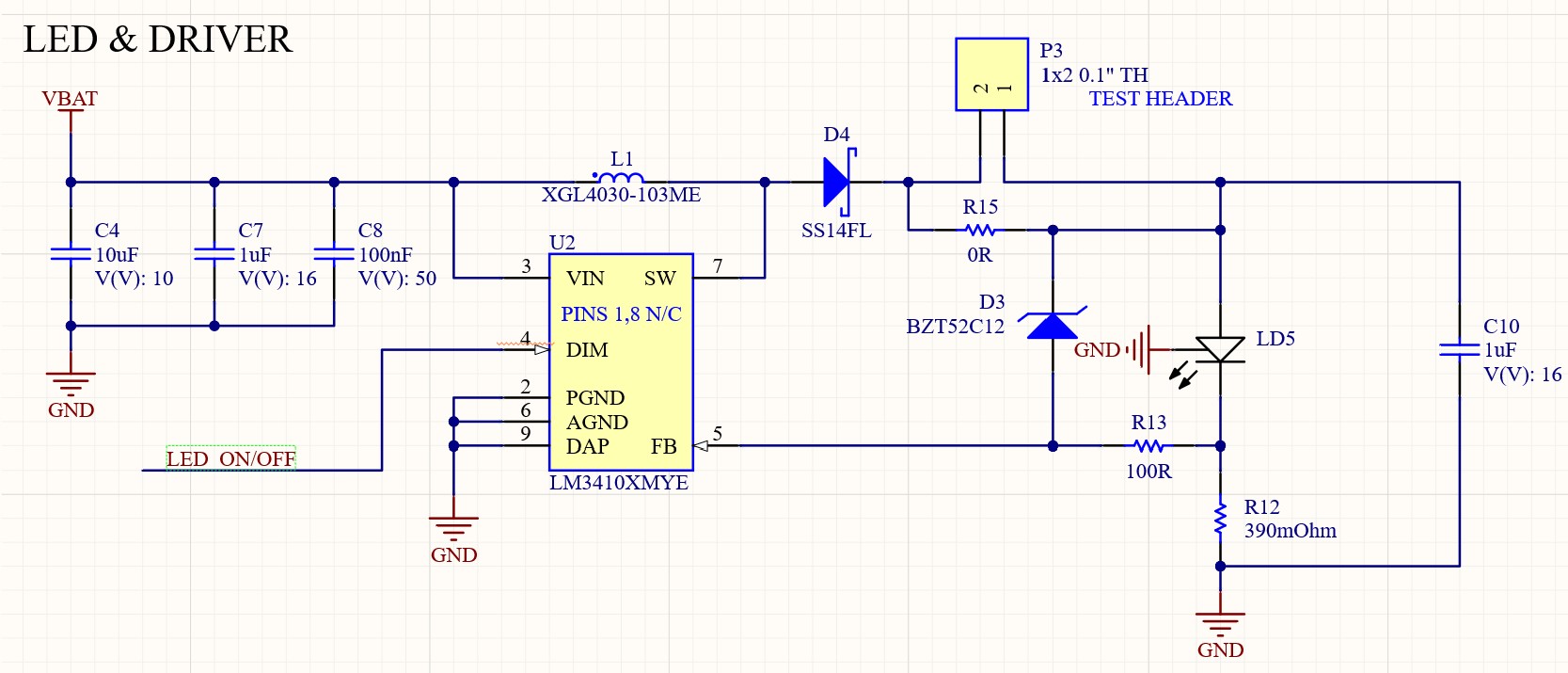
I am having issues getting this circuit to behave as expected.  I have checked for shorts between each of the pins, and that seems OK.  Vin = 3V with Vf(min) = 5V for the LED.  For now, the protection circuit has been removed (R13 = 0R, D3 is removed).

I notice that Vled measures as 5V (so it is boosting) but the current draw isn't right.  With Rfb=390mOhm I would expect that Iled=500mA.  But I'm seeing a total current draw of 120mA, including all the other circuitry on the board.  So something isn't working right.  And I measure about 15mV at pin 5 (FB).  I believe that should be around 200mV.  How could that be lower?

P3 is a 2-pin jumper, right now shorted out.  Eventually, I'll use that to verify the LED current.

Here is a screenshot of the schematic:

Below is a scope shot of the inductor voltage (pin 7):

Any pointers on where to look to figure out why the current isn't right?

James.

  • Images didn't get pasted in.  Here they are again...

    Inductor Current:

    Schematic Snippet

    And R15 is NOT installed...

  • Hello,

    Are you measuring fb from the IC GND to pin 5?  Have you looked at the input voltage to make sure it is not drooping?

    The switching frequency is below 800 KHz, something isn't right there either.  Does you layout have a solid ground plane?

    What is the ground connection on the LED?  If that is the heatsink pad check to see if it is isolated.

    I don't see anything wrong schematic wise.

    What is LED ON/OFF doing?

    Best Regards,

  • Yes, measuring FB to GND measures about 15-20mV when the device is on.  LED_ON/OFF is generally static, though there is a case where it's on for 4 seconds then off for 4 seconds.  Driving with GPIO of MCU, going pretty close to rail-to-rail when driven.

    Yes, all routing on top layer.  Bottom layer is solid GND.  5 GND vias on center pad  to get heat to 2oz bottom plane, though there isn't much of that right now.  The LED seems to be connected correctly with GND connections actually connected to GND.

    Right now I am powering from a power supply with current limit set to 1A.  Just tried setting the current limit to 2A, in case there was some sort of spike of current required.  But same behaviour -- takes about 100mA @3.5V, where it should take somewhere around 2.5-4W for the LED (0.5mA @ 5-7V).

    I double checked the pinout in the routing, to make sure pin numbers didn't get messed up on the PCB, but that all looks good too.

    James.

  • Hello James,

    On the LED there is a ground connection per the schematic.  The anode and cathode are not tied to ground that's what I was asking, is the GND connection isolated from the other two connections?

    You can try increasing the input voltage to 4V or so just to see if it behaves different.  Are you measuring the voltage at the input of the LM3410?  How is the supply connected to the board?

    Are you using an oscilloscope to measure FB or something else?

    Best Regards,

  • Hi Irwin,

    Yes, that middle connection on the LED is a thermal pad that is electrically isolated from the rest of the part.  Right now the LED is right off the board, soldered with wires, so the middle pad is not connected at all.  So that's not involved here I don't think.

    I tried bringing VIN all the way up to 5V without any real difference in results.  I thought if maybe the inductor was saturating and that a higher input voltage would reduce the current required.  But no luck.  And yes, I am measuring at the input of the LM3410.  The cable to my power supply isn't too long or skinny, and distribution on the PCB is good, certainly good enough for just ~1A expected in worst case.  But good question.

    I've measured the FB with both oscilloscope and multi-meter.  Both give values around the same value.

    And I've confirmed that I have the part I think I do soldered on. The markings are SSXB which, according to the datasheet, is the LM3410XMY that I intend.

    Attached is a scope shot of the FB node, with very short ground loop so as to not induce extra ringing.  This is with DC coupling, so you can see the average is about 23mV, but there is a very definite noise pattern:

    Strange indeed.

  • I should mention, that this last scope shot was with a 6.8uH inductor that is rated up to 3.9A (XAL4030).  It has a higher current rating then then 10uH I was using and I think that's a better value anyways.  But I still can't get more than about 100mA out of it and the FB voltage is messed up.

  • I just removed the LED, R12, and R13 and confirmed that the FB node is not shorted to GND (hard to tell with 0.39 ohm resistor).  Then soldered back on the components one by one and ensured there is no hard short.

    Next step is to replace the LM3410.  Maybe I connected or removed P3 jumper live during debugging and fried the circuit ???  Not sure what else to try at this point.

  • Hello James,

    I would recommend turning the band width limiter off though that is not your problem.  I don't think the inductor is saturating, I checked the part and it seemed okay from a quick look.  I may go back and check the part out better since I haven't used that inductor family before.

    The last waveform doesn't make sense from both the frequency and also the wave shape, it should be current ramping up and down, triangular (though that can be from the output capacitor).

    One thing you can try is to increase the current sense resistor value up to regulate a much lower current to see if it starts to regulate and switch at the correct frequency.

    One other thing, is the LED emitting light?

    What is the part number of the LED or if you have the datasheet?  Perhaps the load is an issue?

    Best Regards,

  • So I swapped out the LM3410 with a new device and things make a lot more sense.  Turning on the LED causes Vf~7.5V (which is expected) with a current draw at the power supply of ~1.2A (so ~4.5W).

    My conclusion is the LM3410 device was damaged.  Likely from dynamically removing the jumper while the LM3410 was on.

    Thanks for your help.

  • Hello,

    Yes, that would damage the part, hence the OVP zener for OVP protection.

    Best Regards,

  • Hello Irwin,

    How can I prove that the zener OVP circuit is properly sized?  Vf(max) is 9V and I have a 12V zener in place now.  That seems like it should be size about right with Vz(min) = 11.4V and current starting to flow just under 11V reverse voltage.  So the zener should kick in above any valid voltage for the LED but well below the max voltage of the part.

    Is that a good analysis?

    James.

  • Hello James,

    Sure, however all you are trying to prevent is OVP, you could move it up to a 15V or 18V zener.  If any current flows during normal operation it will cause an offset.  This requires looking at the zener current versus voltage graph and taking tolerance into account.

    Best Regards,