Hi,
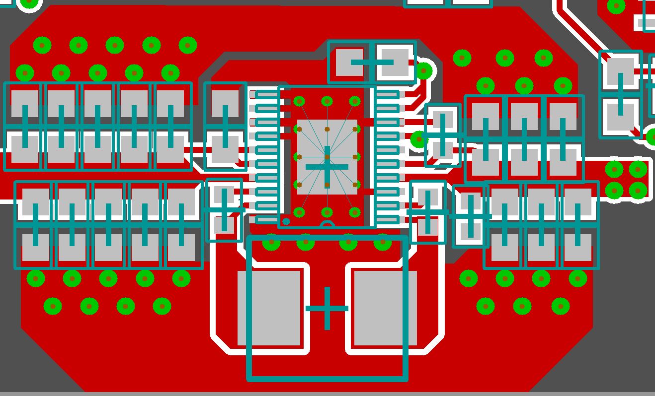
since my last layout for the TPS55165-Q1 didn't work well, i'm trying to develop a new layout. Regarding the layout of the TPS55165Q1 in almost all threads are mentioned the pcb layout of the evaluation board and the application note SLVAEJ2. Due to the difference between the layouts of the evaluation board and the layout of fig. 4 and 6 from the application note, I do not know which layout i should consider for my own layout. So should i rather use the layout of the evaluation board or the other one? In my opinion the design mentioned in the application note manages the PGND and GND connection better than the evaluation board, because the analog ground is exclusively connected to the power ground by the power pad.
In order to achieve a good performance I should consider at least two solid GND copper planes in addition to the quite solid gnd area on the side on which the TPS55165Q1 is placed, am I getting this right?
Best regards,
Tom