This thread has been locked.

If you have a related question, please click the "Ask a related question" button in the top right corner. The newly created question will be automatically linked to this question.

TPS2511EVM-141: Snubber Circuit to reduce EMI

Part Number: TPS2511EVM-141
Other Parts Discussed in Thread: TPS54240, , TPS2511

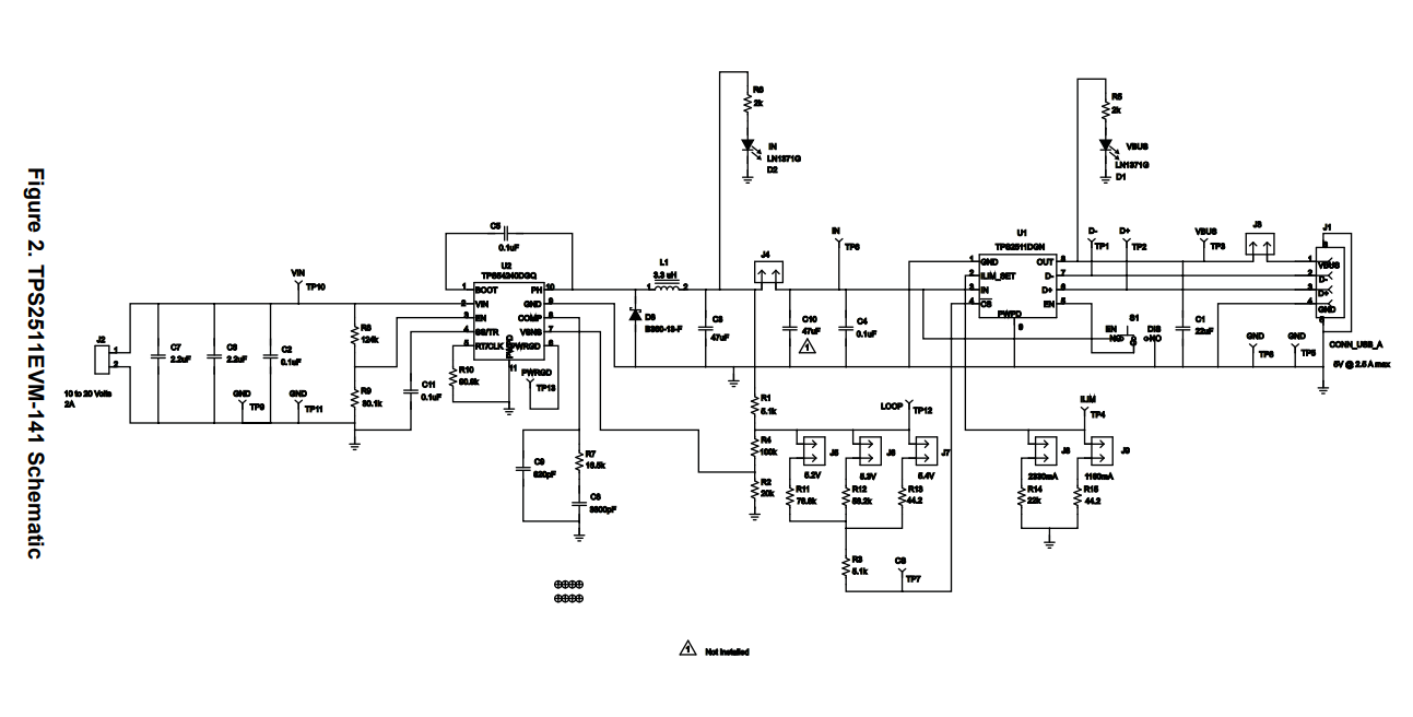
I utilized the TPS2511EVM-141 components and layout in a design with a BLE connected device and the Circuit is failing radio emissions testing due to EMI created by the switching regulator, TPS54240. 

On the EVM board there is a flyback diode, D3. In other designs I have seen a snubber circuit utilized in parallel with this diode to minimize any ringing that may occour.

I would like to know if there are any recommendations for values of a capacitor and resistor series to go in parallel with D3 as a snubber circuit for use with the components and respective values in on the EVM board that will effectively reduce ringing on the output of the TPS54240 and minimize EMI.

 See attached Data sheet, schematic on PG 4.

Thank youTPS2511EVM-141.userGuide.pdf


  • Hello,

    D3 on the EVM is a Schottky diode, and on this system, it is used to prevent the possibility of large ground currents into the TPS2511 during sudden disconnects due to inductive effects in a cable.

    I do not have any recommendations for a snubber circuit to help with EMI as the TPS2511 is just a load switch and not designed to reduce EMI from upstream devices. I recommend reaching out to the TPS54240 team to see if they have any recommendations on a filter or how to make the output of the TPS54240 more stable. Post a new question, but put the TPS54240 as the part in question. This will assign it to the proper team.