


Hi TI,
I have several questions on UCC25640x Design Calculator as below.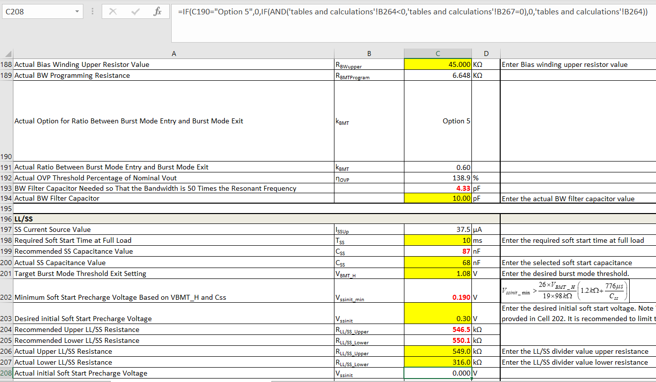
- For LL/SS, why actual Vssinit in cell - 'C208' is 0V? Although it is Option 5 where LL/SS pin is pulled down by internal 1.2kOhm, it should not get 0V. With 13V of Vrvcc, the actual Vssinit = 13 x 1.2k//316k / (1.2k//316k + 549k) = 0.0282V.
- Can you enable the "table and calculation" tab? I am in a 'black box' in LL/SS calculation.
- Issup value in cell - 'C197' is 37.5uA while it is 36uA in its datasheet. Which value should we follow?
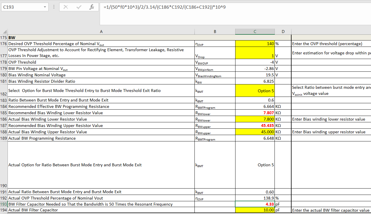
4. Equation in cell - 'C193' involves actual OVP value, which is incorrect, right? The actual OVP value in cell - 'C192' should be the Upper resistor value in cell - 'C188', right?
5. Would it be OK if switching frequency at no load based on Mg_ꚙ on Mg vs fN curve is more than maximum switching frequency since it would enter burst mode at low load?
6. Is UCC256404 max switching frequency 350kHz?
Regards,
KK


