Other Parts Discussed in Thread: PMP40294, BQ3060
Hi TI engineer,
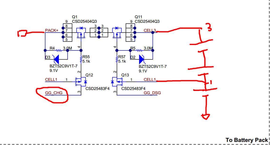
I am in a puzzle about the schematic in PMP40294 Reference Design Board.
It's protect circuit has NetLable named GG_CHG and GG_DSG, they don't have a corresponding lable in the schematic.
Could you please explain a little about the working principle of the circuit in the picture below?
especially why choose the CELL1 as the Q12's Grid, and how GG_CHG or GG_DSG refluce the charge and discharge process.
Thanks a lot!