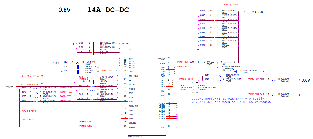
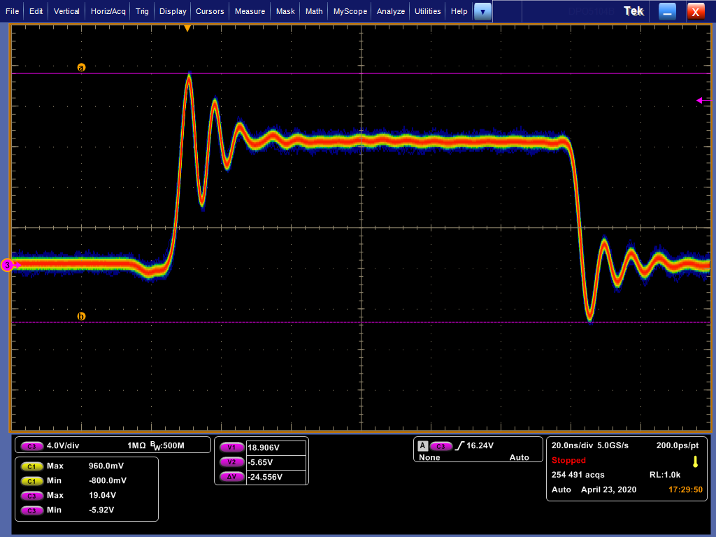
The equipment we use is as follows ~~
Tektronix P5205A-2 High Voltage Differential Probe 100MHz 50X Bandwidth no limit
Oscilloscope: Tektronix DPO5104B 1 GHz digital 4 ch Bandwidth: 1GHz
This thread has been locked.
If you have a related question, please click the "Ask a related question" button in the top right corner. The newly created question will be automatically linked to this question.
While this is unlikely to cause damage, it is always recommended to keep the device within its listed datasheet maximums.
Yes, you can use a snubber from the SW not to PGND node. I would recommend starting with a 1nF snubber with a 1-Ohm resistor and working from there. Layout of a snubber is critical to keep the loop inductance as short as possible so that the snubber is effective at ~120MHz where this ringing is occurring.
A small, ultra-fast rectifier diode directly between the SW node and PGND may be able to react fast enough to shunt some of the current and reduce the negative peak, but I would not recommend a TVS diode as a TVS diode is unlikely to react fast enough to provide much peak suppression
You can also try changing C29 from 100nF to 10nF. These smaller capacitor values in 0402 packages offer lower ESL and the ability to suppress higher frequency noise. We have seen significant SW ringing improvement placing a 2.2nF - 10nF 0402 capacitor from VIN to GND under the VIN pins on the backside of the board when there are vias available to connect VIN and the thermal pad to the backside of the PBC. By providing a separate, parallel path from the main power path, this helps reduce the inductance and high-frequency performance of the bypassing.
Hi SIR
You can add a resistor upto 4.7-ohm in series with the boot strap capacitor (C311 in your schematic) to slow-down the turn-on of the high-side FET and reduce overshoot ringing on the SW node on its rising edge, but the turn-off of the high-side FET does not drive current through the BOOT pin, so it will have minimal effect on the speed of the turn-off. With an external FET controller, adding a resistor in series with the gate drive signal would help reduce the turn-off rate, but with internal drivers and FETs, there is no access to the FET turn-off driver path.
You can try replacing D25 with a high-speed rectifier diode, or an R-C snubber to reduce the negative peak on the falling edge of the switching node.