This thread has been locked.

If you have a related question, please click the "Ask a related question" button in the top right corner. The newly created question will be automatically linked to this question.

TPS53915EVM-587: Non-matching between schematic and layout on the TPS53915EVM-587 board

Part Number: TPS53915EVM-587
Other Parts Discussed in Thread: TPS53915, TPS53317A, TPS53317

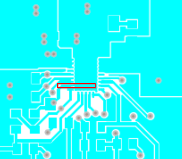
Q1) I found that in the schematic is AGND (pin 22) connected to PGND via resistor R8 = 0R but in the top layer, I saw that pin 22 (AGND) connected directly to IC's Thermal Pad. So that I get confused about this connection. Which one is correct?

Q2) Can R8 change be to ferrite bead? and Can you recommend the part number?

I also attached the picture for more details.

Thanks a lot

Tuan Le 

  •  

    Q1) I will check on why the schematic and the layers are out of SYNC.  They Layout appears to be using a "net-tie" to directly connect the pin to the thermal pad without using a resistor.  This is preferred over connecting the AGND pin to the thermal pad through a resistor.

    Q2) R8 (AGND to PGND) should not be a ferrite bead.  The high impedance at high frequency between AGND and PGND could interfer with the IC's functionality as digital signals cross from the Analog Ground to Power Ground domains within the chip.

  • Dear Peter

    Thank you for your reply soon

    I have another question according to Q1.

    In my project I already used TPS53915 to convert from 12V to 1.8V/7A. But when I measured signals as power good, SM Bus and Address pins then I saw that they have some noise. After check layout in my board, I see it different with TPS53915EVM-587 at pin 22 connected directly to thermal pad. I asume that this is reason why my board have noise. If correct, could you explain this one?

    I will explain about layout in my board, I drew pin 22 (AGND) via from Top layer to Bottom after that connect to resistor R8 = 0R to PGND at bottom and via from bottom to Top layer to connect to IC's Thermal pad.

    I also attached picture for more details

    Thanks

    Tuan Le

  •  

    The 3 digital outputs of the TPS53915 (SDAT, ALERT, PGOOD) all use Open-drain output stages.  When their internal pull-down FETs are active, they short the pin to their local ground.  Due to the high current flowing through the ground at the IC, there can be some noise between this ground point and a ground point sensed elsewhere on the PCB.  This is normal, and expected, and should be well below the I2C/SMBus specified minimum deglitch filtering of 50ns for the PMBus transmission, so it should not affect operation.

    I would not expect this to improve or "go away" by connecting the AGND pin directly to the thermal pad on the top layer.

  • Hi Peter

    I already have checked Power Good waveform in TPS53915 datasheet, I saw that there is no noise on Power Good signal with bandwidth of probe is 20Mhz. I tried this one on my board and saw that the power good is lose noise. But If I changed the bandwidth of probe to 250Mhz or 500Mhz is appearing noise. Could you please explain the different between selection bandwidth of probe? Why did you measure the signals in the bandwidth 20Mhz?

    I attached the picture TI's waveform and my waveform in below

    Thanks you so much

    Tuan Le

  •  

    Oscilloscopes have the ability to apply a bandwidth filter on their input signals to reduce very high frequency noise that can be picked up by their high-bandwidth probes.  The frequency is the 3dB (half-power) point of the single-pole filter.

    We routinely select a 20MHz bandwidth filter when measuring low-band width signals for generating oscilloscope waveforms to remove induced measurement noise from the images to make them more readable.  Oscilloscope ground clip loops, multiple ground connections on the PCB, especially when measuring a highly dynamic signal like SW that is switching from 0V to 12V in a few nanoseconds, can induce a lot of measurement noise, selecting bandwidth limiting removes these artifacts from the signals and makes the signals of interest easier to read.

    In the case of PGOOD, when the PGOOD signal is low, the PGOOD pin is shorted to GND inside the TPS53915 with a low-resistance FET, so PGOOD is tracking the ground of the TPS53915.  This ground has a lot of high-frequency noise on it with respect to where you connected your ground clip because the GND is also carrying a lot of dynamic switching current from the Power FETs, so when it's low, you see noise on it, but once the pull-down FET is released to be pulled, you don't see that noise.

  •  

    I see that you have selected "reject" on this threat.  Can you please help me understand what about my explanation you have rejected?  And what additional details you need me to clarify to help you?

  • Hi Peter

    Thank you so much for your detail explanation and providing clarification on my queries. It helps me to more understand about the noise in TPS53915.

    About click "reject" on this threat. That is my mistake. Sorry about that.

    Thanks

    Tuan Le

  • Hi Peter

    I would like to ask another question regarding to noise in the power good signal.

    I tried to measure the power good signal in TPS53317A (FET-integrated) with setup limit probe bandwidth at 250Mhz but I did not see any noise in this signal. Could you please explain about the different between TPS53317A and TPS53917? Why the power good signal of TPS53317A have not noise in it.?

    I also capture power good signal waveform of TPS53317A at below.

    Thank you so much.

    Thanks

    Tuan Le

  •  

    The TPS53317A and the TPS53915 are built in different package technologies and have very different MOSEFT structures resulting in different ground noise levels with respect to an external ground.  The TPS53915's PGOOD pin has a lower impedance to its PGND than the TPS53317A, which filters the PGND noise from appearing on the PGOOD pin.

    The difference between the TPS53317 and the TPS53317A is there minimum operating output voltage.  The TPS53317 has a minimum operating output voltage of 0.6V while the TPS53317A is designed to be able to operate with reference inputs down to 0.9V and output voltage down to 0.45V for lower voltage DDR memory.

  • Hi Peter

    Thank you for your explanation.

    So now, could you help me to find any solutions or workarounds for increase impedance between PGOOD pin and PGND on TPS53915? and I'd like to request more documents or errata which one show lower impedance will cause the noise on PGOOD pin. Please send it to me.

    One more things, could you please suggest an alternative part for TPS53915? we hope that they have pins compatible.

    Best regards,

    Tuan Le

  •  

    The low impedance of the internal PGOOD pull-down MOSFET and low impedance from the MOSFET's source to the power ground of the TPS53915 combined with the very low output capacitance of the PGOOD pin causes the PGOOD voltage to follow the PGND of the TPS53915 very closely.  While this ensures the lowest possible voltage at PGOOD with respect to PGND, it can allow PGND noise to appear on PGOOD.

    The most common technique for filtering PGND noise on PGOOD is to add a small series resistor to the PGOOD signal with a bypass capacitor local to the receiver of the PGOOD signal.

    There is no alternative part to the TPS53915, nor is this a "bug" that requires an application note or errata.  The PGOOD function is working, the issue is differences between the ground voltages at the TPS53915 and the receiver it is being monitored at.

  • Hi Peter

    Thank you so much for the help you gave me all the time. I greatly appreciate the assistance you have provided me.

    Thanks

    Best regards,

    Tuan Le