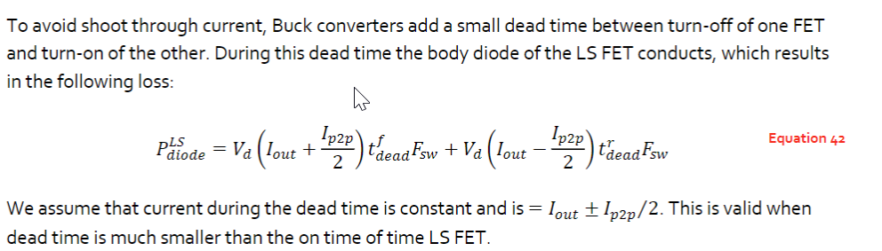
This thread has been locked.

If you have a related question, please click the "Ask a related question" button in the top right corner. The newly created question will be automatically linked to this question.

TPS546A24A: Schottky diode

Part Number: TPS546A24A

Hi,

Would adding a Schottky diode between the switch node and ground help improve efficiencies in the regulator (to allow current to conduct before bottom fet turns on)?  There is a body diode on the bottom fet that would conduct instead but as far as I understand that diode is probably not a schottky diode.

Thanks

  • Hi Daniel,

       It really depends on the dead time of the converter. You can run simulations to estimate the voltage drop during the dead time and estimate power losses due to dead time. Then you can estimate the losses by using a schottky diode and then get an understanding of the power savings from using the schottky diode.

    The loss equations are given below.

    regards,

    Gerold

  • Hi Gerold,

    Is there a simulation tool for the TPS546A24A available?   That is the device I am specifically using. I saw there are spice models but they appear to be encrypted.  Do you happen to know for this regulator if a parallel Schottky diode improves efficiency?  The dead time is actually specified on the datasheet but the Vd is not.

    Thanks,

    Dan

  •  

    The dead-times of the TPS546A24A are extremely short, and the forward drop across the body diode of the internal FET is quite low, between 0.5 and 0.7V under typical current loads.  Between the very short dead-time and the low forward drop across the body diode, and the package and layout inductance required to move the current between the MOSFET channel, and external diode, and back, there is very little benefit to adding a Schottky diode between PGND and SW in a real application.

    Simulations may show a very small improvement because the simulation models do not include the package inductance for the TPS546A24A or the Schottky diode, but real circuit measurements will show very little to no benefit.  In fact, if adding the diode to the layout increases the conduction path from the SW pins to the inductor terminal, it may actually show a lower efficiency as the added trace resistance loses, combined with the additional leakage losses when the diode is reverse biased, and the capacitive losses charging and discharging the diode's junction capacitance, can be greater than the savings from the body diode conduction.