This thread has been locked.

If you have a related question, please click the "Ask a related question" button in the top right corner. The newly created question will be automatically linked to this question.

TPS7A7100: About Input Capacitor Requirements

Part Number: TPS7A7100

Hi,

Customers use TPS7A7100 under the following conditions:
・Vin=3.3V, Vout=3V, Iout≒300mA
・Cin:0.1uF, Cout=10uF, 1uF, 0.1uF (ceramic cap), Cff=0.1uF

In the above situation,
Output oscillation occurred which is thought to be caused by the input side.
Customers are trying to improve on the following in their data sheet:
I got three questions from a customer about datasheet ”About Input Capacitor Requirements”.

1.Could you tell me the mechanism or principle of TPS7A7100 oscillation in the following cases?
"For example, a 5-nH inductor and a 10-µF input capacitor form an LC filter that has a resonance at 712 kHz.
This value of 712 kHz is well inside the bandwidth of the TPS7A7100 control loop."

2.Please tell me the target of resonance frequency by C and L.
   Customers want to know the resonance frequency that should not be exceeded.

3.The typical characteristics were acquired under the condition of Cin = 10uF.
   In this case, what is the assumed inductance due to the PCB, etc.?


Could you give me your advice?
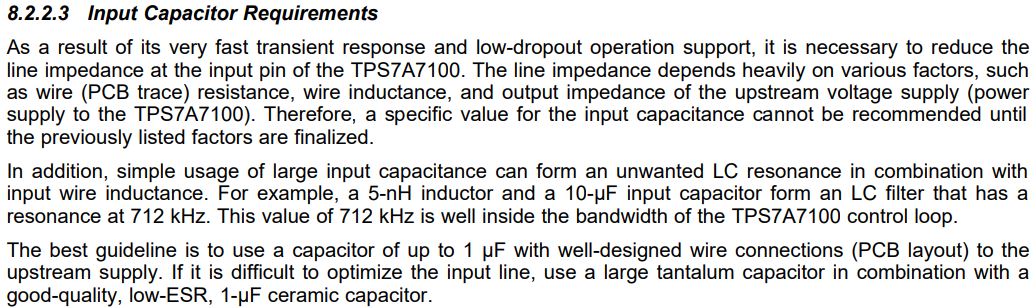

Regards,
Yusuke


  • Hi Yusuke-san,

    I've added my answers in green. 

    1.Could you tell me the mechanism or principle of TPS7A7100 oscillation in the following cases?
    "For example, a 5-nH inductor and a 10-µF input capacitor form an LC filter that has a resonance at 712 kHz.
    This value of 712 kHz is well inside the bandwidth of the TPS7A7100 control loop."

    LC circuits (think about an LC Tank ) can resonant if there isn't enough resistance to dampen the ringing. When this happens on the input of a regulator it can cause the regulator output to ring for a few reasons 1) it could be that the input is drooping enough to put the LDO into dropout, which will force the output to go low and then will recover when the input increases. 2) If the ringing on the input is near the bandwidth of the regulator's unity gain bandwidth then both the LDO control loop and the input voltage are changing at similar times and each one effects the other so the two interact with each other (an example is when Vin goes up, the LDO must make the pass device more resisitive to keep the output from increasing)  


    2.Please tell me the target of resonance frequency by C and L.
       Customers want to know the resonance frequency that should not be exceeded.

    Like most modern LDO's this device's control loop bandwidth scales with load current and ranges from approximately 100kHz to 1MHz (between light load and full load). In general the safest thing to do is to ensure that the ringing on the input is at a frequency that is ten times smaller or ten times larger in order to keep the interference with the control loop negligible. If you can't keep the LC resonant frequency outside the control loop then there needs to be some resistance to dampen the ringing so it doesn't turn into a full oscillation. 


    3.The typical characteristics were acquired under the condition of Cin = 10uF.
       In this case, what is the assumed inductance due to the PCB, etc.?

    The inductance is low for our characterization boards which have wide power traces (to minimize inductance and resistance) we usually estimate that they have approximately 1nH of inductance. This would have a resonant frequency of approximately 10MHz. 

    I hope that helps.