This thread has been locked.

If you have a related question, please click the "Ask a related question" button in the top right corner. The newly created question will be automatically linked to this question.

TPS63020: Need help reviewing Buck Boost design for TPS60302

Part Number: TPS63020

Hi,
The following are the design parameters

Vin: 3.3V to 4.2V (Li Ion Battery)

Vout: 4V
Iout: 2.5A

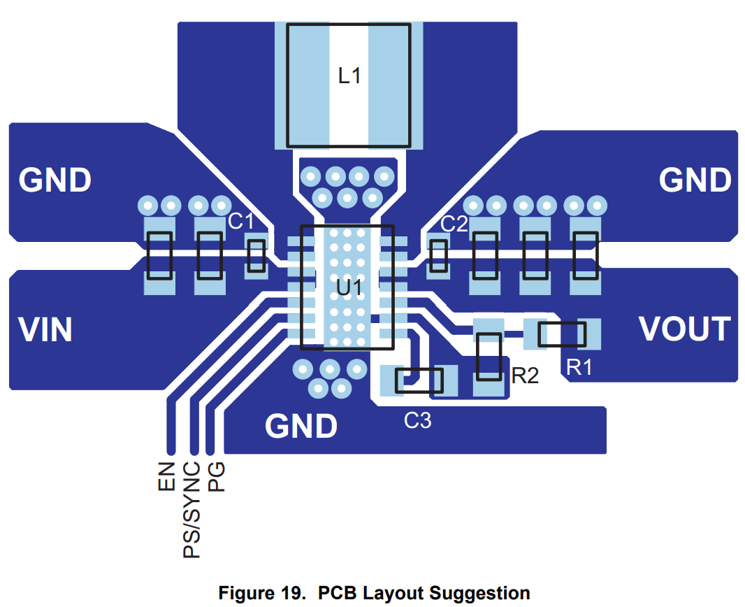
Following is the schematic and PCB design . Need help reviewing this design and any insights as to how it could be made better

Thanks!

Milind
Hardware Engineer
PupilMesh Private Limited


  • Hi Milind,

    Thank you for reaching out.

    The schematic looks fine. For the PCB, you need to do the following changes:

    1. Move the input and output capacitors as close as possible to the IC.
    2. Add more GND vias close to the PowerPad of the IC and close to the GND ends of the input and output capacitors.
    3. Connect the GND end of C29 to the GND pin.

    This is the recommended PCB layout, please try to follow it as close as possible:


    A proper PCB layout is extremely important for swithmode converters. Here are some application notes on PCB routing, the same applies to the buck-boost converters:
    http://www.ti.com/lit/pdf/slyt614
    http://www.ti.com/lit/pdf/slva773

    Best regards,
    Milos