Because of the Thanksgiving holiday in the U.S., TI E2E™ design support forum responses may be delayed from November 25 through December 2. Thank you for your patience.

This thread has been locked.

If you have a related question, please click the "Ask a related question" button in the top right corner. The newly created question will be automatically linked to this question.

LM2585: Is it working correctly or is it behaving erratically?...

Part Number: LM2585

Hello everyone,

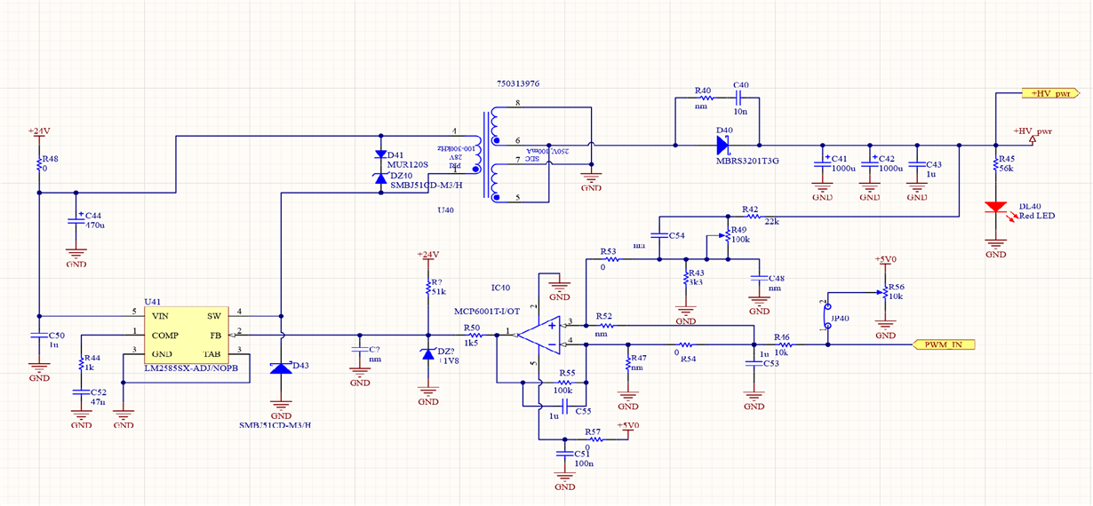
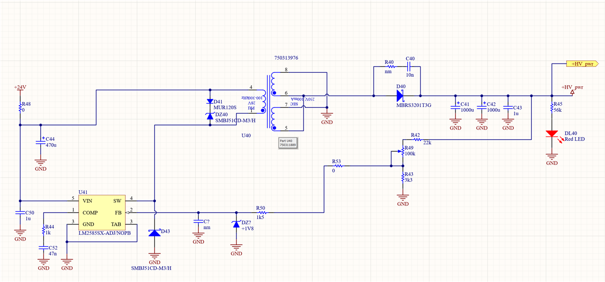
I am attaching the schematic diagram of the circuit it is giving me headaches:

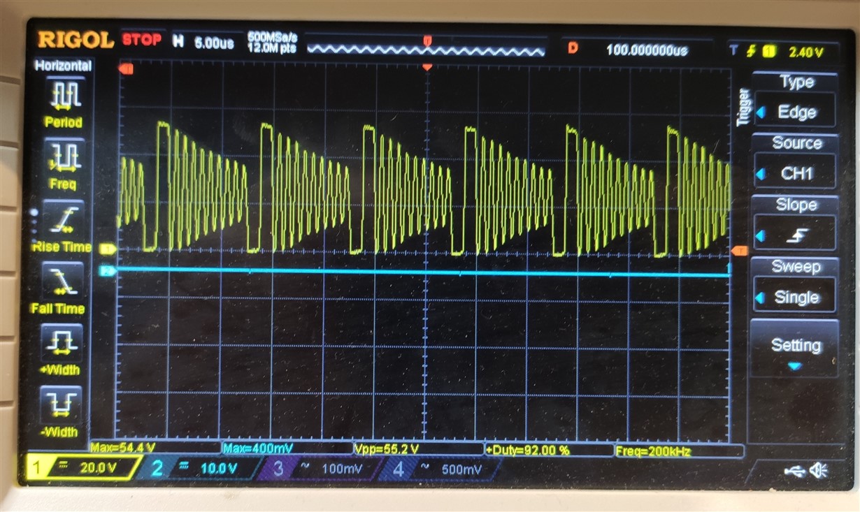
Essentially it is a flyback converter which takes the +24V at the input and raises it, with the aid of a 750313976 tranformer by Wurth Electronics, from 0 to +60V depending on the PWM IN duty cycle. The output is substantially a capacitor of a few uF which is switched on and off at around 50 to 100 Hz (not shown in the schematic). What surprises me is the waveform at the "switch" pin: in all cases it is discontinuous (which might not be a problem per se), but it is the fact that "wanders" which puzzles me (you can see it in the following video):

The result of this, is that the power read at the PSU is unstable, as you can see in the following video (first line PSU voltage, second line current, third line power):

I am also attaching a few extra pictures:

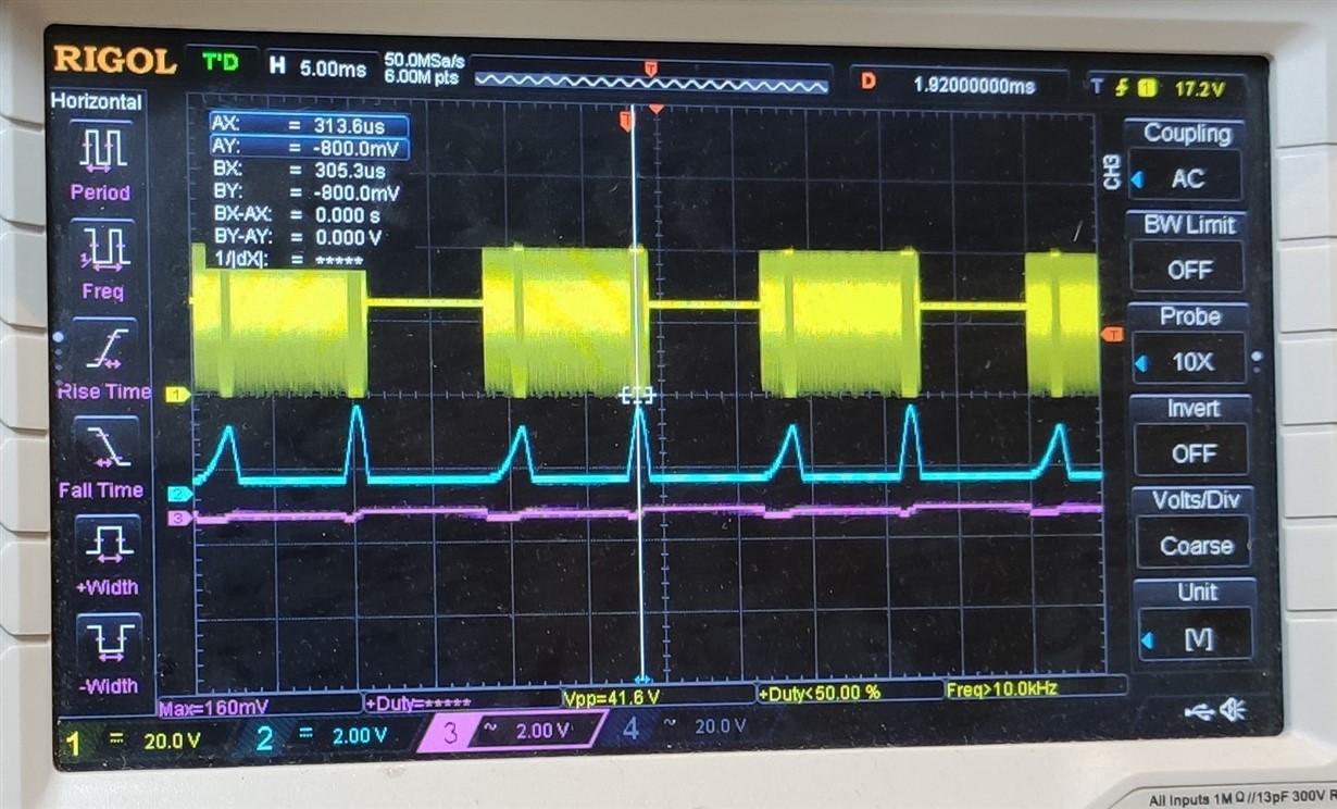
Picture "2"; yellow = SWITCH pin, blue = COMP pin, purple = output voltage AC coupled (to see output ripple)

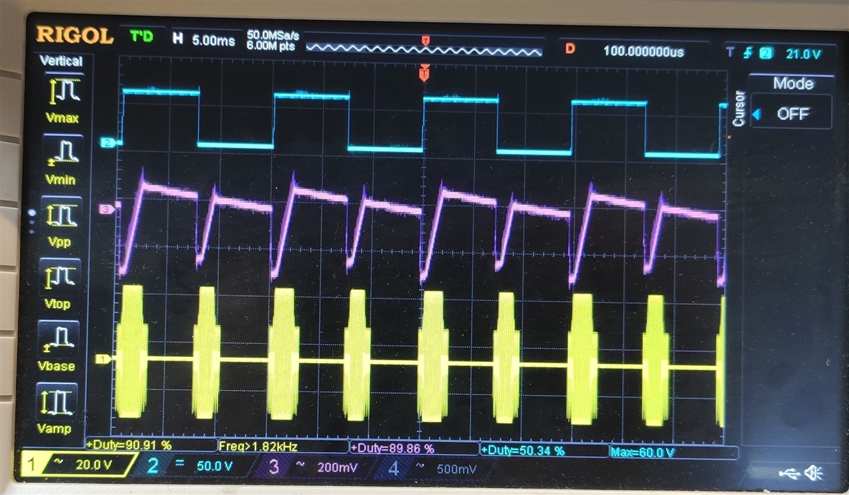
Picture "5": yellow =SWITCH pin, blue = 60V output; ; purple = output voltage AC coupled (to see ripple);

Picture "6": yellow =SWITCH pin, blue = 25V output purple = output voltage AC coupled (to see ripple);

Picture "ringing": at the SWITCH pin, this is what appears most of the time.

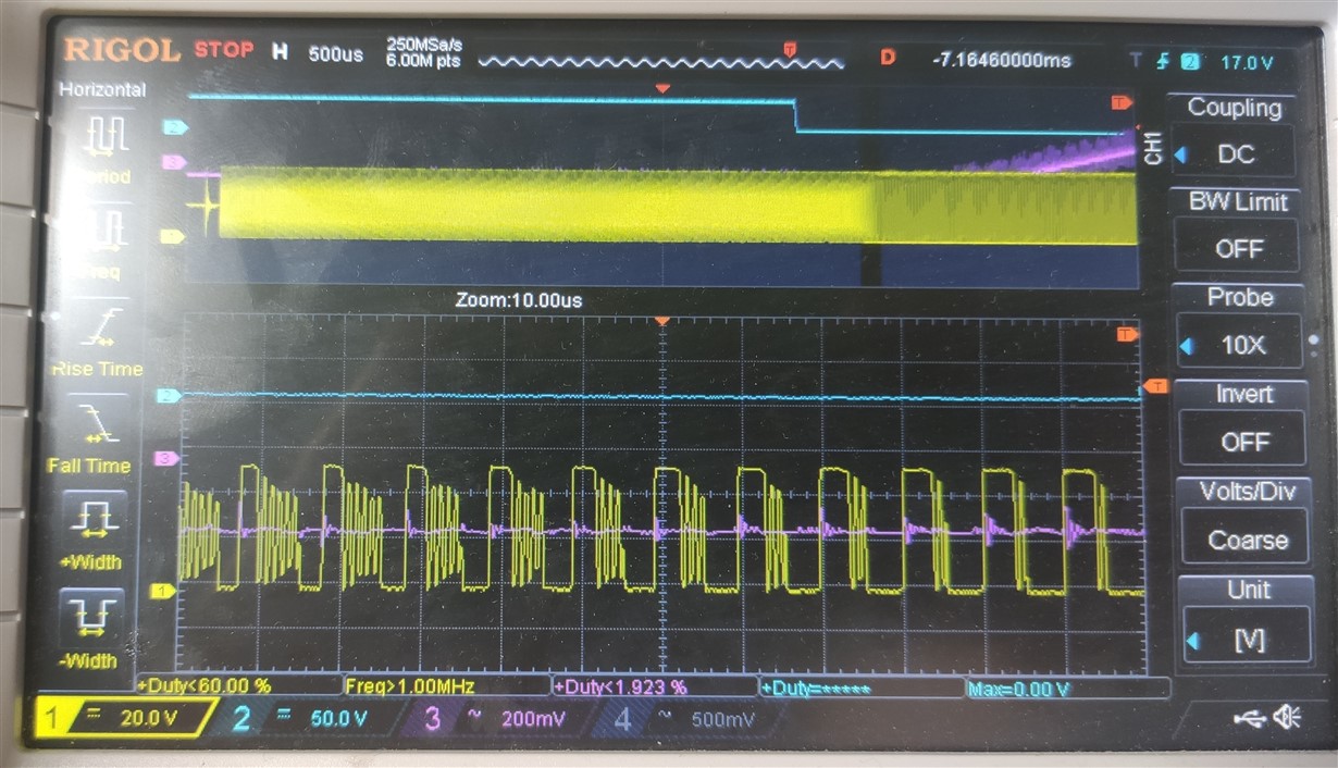
If I zoom in at the SWITCH pin there where the COMP pin is higher (see pic 2), it so happens what is detailed in the "ringing zoomed" picture: the positive pulse appears to widen a little and the ringing tends to disappear:

Am I doing anything wrong? Except for these strange pictures and the power readings (well, and a little whining from the transformer from time to time), the system appears to be working well, however I would like to know if I am mistretaing the LM2585 to that reliability or EMC emissions are out of spec.

Thanks,

Paolo.


  • HI Paolo,

    Thank you for designing with the LM2585.  Our experts supporting this device are currently on holidays, and they will be back to work later this week. 

    I took a look of your schematic and it looks complex.  The output can be directly sensed with a resistor divider at the FB pin,  so I don't understand why you employ an external op-amp.  If you want to adjust the output voltage, your control signal PWM-IN can feed to the FB through a resistor.  

    Basically the loop is not stable. Please remove the op-amp circuit and use the internal error amplifier directly for a simple loop compensation.  Also check your transformer inductance, which may need to be increased if you want it to operate to CCM.


    Thanks,

    Youhao Xi, Applications Engineering

  • Hello Youhao,

    thanks for the reply. As a matter of fact, I had already tried what you suggest (I eliminated the PWM for the test), but things are not that different:

    This is the simplified schematic which generated the above picture:


    As for the transformer, the one I am using has around 47uH, as suggested by the datasheet, but I also tried bigger and smaller ones with no success...

    How can you say it is an unstable loop?

    Thanks!

    Paolo.

  • Hi Paolo,

    I just realized that the purple curve is 500mV/div, on top of 50V rail.  This is just 1% ripple voltage.  Its pretty good for a switching mode power supply. 

    Can I ask you how do you select the resistor and capacitor for the COMP pin?  Can you raise R44 by 10x but reduce C52 by 10x and see if there is any improvement?

    Thanks,

    Youhao

  • Hi YouHao,

    yes, I tend to agree, the cicuit behaviour is good overall... I am pretty happy about the output, it is the input which worries me...

    Here are the modifications you requested:

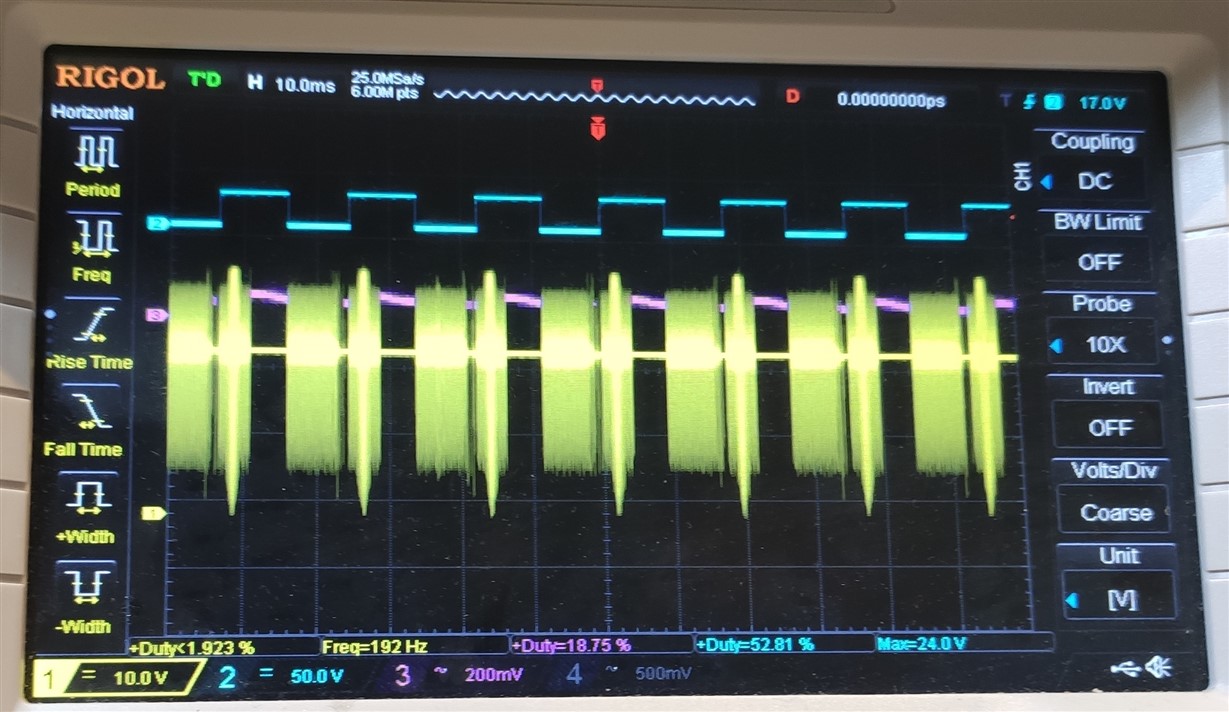
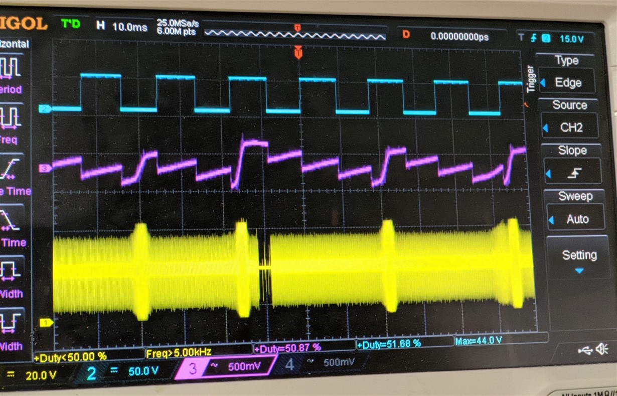
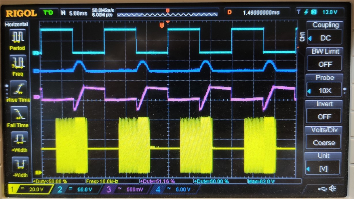
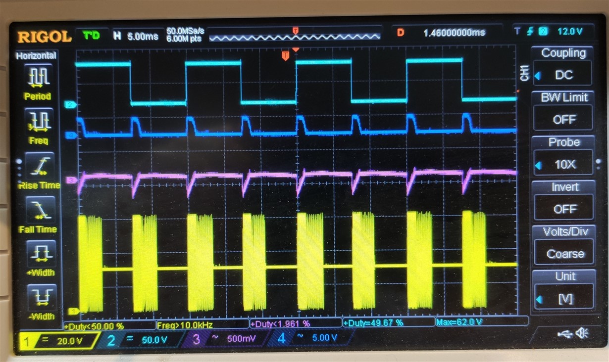
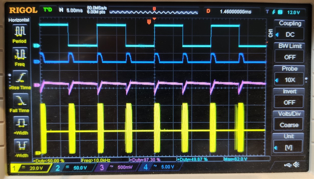
    (light blue = circuit output, dark blue = COMP pin, purple = 60V DC out, AC coupled to show ripple, yellow = SWITCH pin)

    Original configuration (1k+47n):

    10k+4n7 as you requested:

    As a test, I added, in parallel to the 10k+4n7, an additional 1n (directly from COMP pin to ground):

    As for the choice of components, I tried to calculate them starting from your "compensation networks made simple" documents... I might have gotten them wrong, though...

    Which picture do you think is better?

    Thanks,

    Paolo.

  • Hi Paolo,

    Sorry for the delay.  It took awhile in trying to digest the info shown in these scope pictures.  Are you sure CH-4 (blue, 5v/div) is the COMP pin signal? What is exactly the other blue trace (50V/div)?

    Among the three, the last two circuit show faster response, and 2 and 3 are basically the same.  The added 1nF parallel capacitor would help attenuate high frequency noise effects if set properly.   The 3rd picture definitely shows cleaner operation.  

    Thanks,

    Youhao

  • Hi again,

    ye, I am positive: the dark blue trace is the COMP pin. The light blue one, the square wave, is the overall output of my circuit, which includes a MOSFET section (not shown in the schematic I attached) which "slices" the +60V and the result is, as shown, a square wave which is applied to the load.

    So, you would seem to indicate that the circuit in the 3rd picture is working neatly, Am I correct? And the fact that it is working in discontinuous mode is probably the reason why the power consumption read at the PSU is changing rapidly?

    But overall, are you confident that the circuit is working well, reliably and within specs?

    Thanks again,

    Paolo.

  • Hi Paolo,

    Based on what I have seen, yes, the 3rd picture is better than the 2nd.  

    The only thing that bothers me is the similarly response after both the rising and falling edge of your output.  At the big square wave rising edge, you output some power, and the rise of COMP and also the switching is understandable.  At the following edge,  you simply disconnect the output, why the COMP voltage also  jumps up?  Do I miss something?

    Can you monitor the +HV_pwr node voltage instead the voltage after your output switch which you never showed me on your schematic?

    Thanks,

    Youhao

  • Hi Youhao

    Well, dont' be bothered, it makes perfect sense! I did not mention it, but there are two identical loads, one connected to the light blue signal you see and the second one connected to the same signal but 180° out of phase... So in fact yes, there is a surge in power consumption each rising or falling edge!

    The +HV_pwr node voltage is connected to purple trace, it is AC coupled to show ripple but that is the node you are interested in.

    Thanks,

    Paolo.

  • Thank you Paolo for the clarification. 

    Wish you good luck in your project.  Feel free to let use know if you have further questions.

    Best Regards,

    Youhao

  • Thanks, so I can assume the circuit is working ok, right?

    Thanks,

    Paolo.

  • I think so.  

    Best Regards,

    Youhao