Hi,
my customer's schematic is as below:
At normal condition, V1_DRV is 12V, the output VC_boost to VE_boost is 25V. The OUT pin duty cycle is 42%.
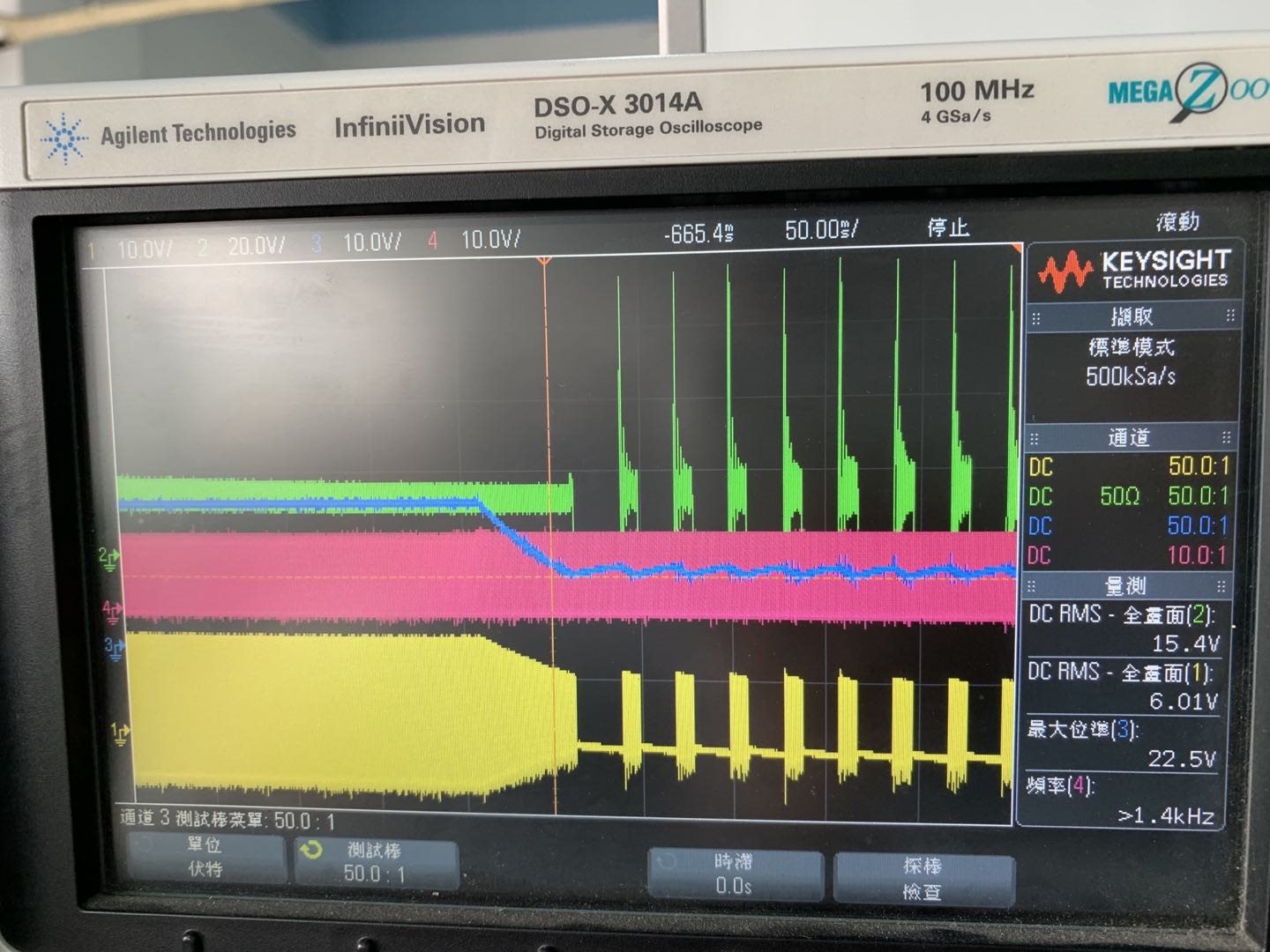
They will observe that the duty cycle of OUT pin decrease to a very low level and VC_boost to VE_boost will decrease to around 10V, since the voltage is given to gate driver which will drive the gate side of the IGBT, low voltage will let the IGBT be in saturation region and burnt out. So it's a serious problem.
Blue line is (VC_boost - VE_boost).
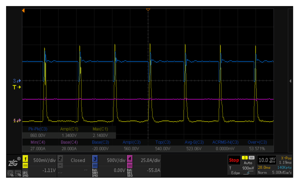
Out pin voltage waveform when ISENSE is 1V is the yellow line below, it's a very low duty cycle pulse, which result in the drop of the output winding voltage.
The question is:
1. why the OUT pin's duty cycle is very low when ISENSE=1V(which represents over current).
2. Are there any way to achieve over current protection(turn off OUT pin) within UC2845?


