Other Parts Discussed in Thread: LM5145, LM5146-Q1
Hello,
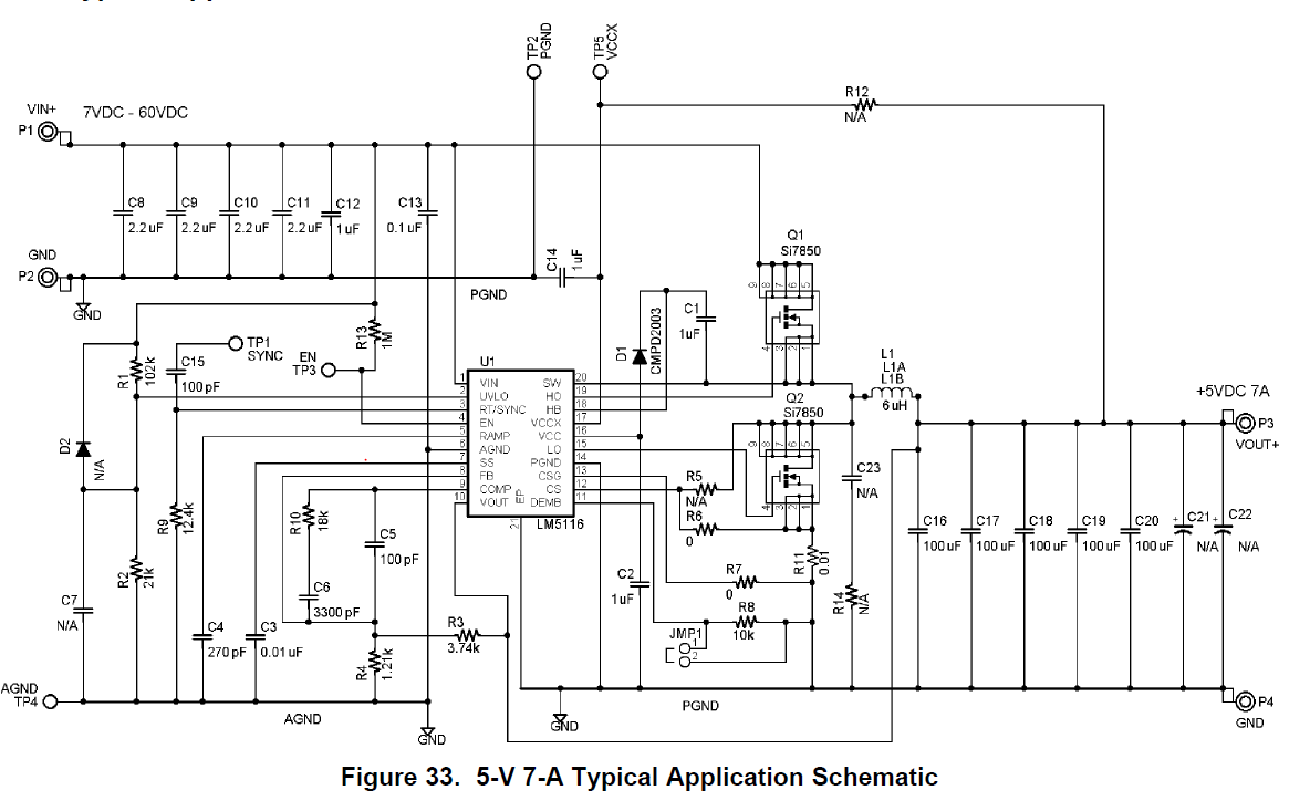
I am new to circuit design and electronics engineering so please bare with me. I am trying to understand the use of LM5116 and attempting to simulate the sample circuit given in the LM5116 datasheet. However I am not sure what to use for the "N/A" components. Do I just ignore and connect a wire there? I am also confused for TP1... does this connect back to the SYNC I/O? If I prove at Vout using OrCad PSPICE probe I should see 5V without adding a resistive load right?
Any help would be great.