This thread has been locked.

If you have a related question, please click the "Ask a related question" button in the top right corner. The newly created question will be automatically linked to this question.

BQ24616: BQ24616 Ground connection

Part Number: BQ24616
Other Parts Discussed in Thread: TPS54334

Hi team,

I would like to ask the meaning about BQ24616's datasheet.

As you can see in Figure 18 of attachment, Analog GND an

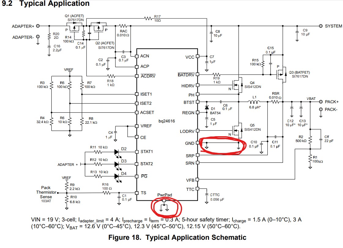
d Power GND has been in chains directly. No part between them(ex. Bead connection).

So, what i want to know is, I wonder if i can connect Analog ground and Power ground directly.

Thank you in advance.

  • Hi Sangha,

       Route analog ground separately from power ground. You can connect analog ground and power ground together using power pad as the single ground connection point, or using a 0Ω resistor to tie analog ground to power ground.

  • Hi Kedar,

    There are two more questions.

    1. What if i do not connect single connection or 0Ω resistor tie?

    2. I don't want to separate analog ground and power ground. My application have to take only one GND because of narrow PCB space. So I am going to tie a REF power to power GND. Does it have any problems if i do not separate Analog ground and Power ground?

    Thank you very much.

  • Hi Sangha,

    1.   If using a 4 layer board, the separate AGND and PGND have to be tied together, and the ideal connection is to use the thermal pad as the single ground connection point. Or you can use a 0-Ω resistor to tie analog ground to power ground (the thermal pad should tie to analog ground in this case). A star connection under the thermal pad is highly recommended.
    2. The issue with one GND is that a solid GND layer is required as you want adequate shielding and as low impedance of a ground path as possible. It would be hard to not route through the bottom trace at all, as this would cut up the uniform PGND layer. Moreover with PGND being the return path for the power stage, the high current carrying PGND could also cause a relative ground shift, and also possibly introduce noise (switching happens relative to PGND so EMI could couple onto AGND if they are shared/same layer) into the analog voltage sensitive pins like VREF, VFB, TS, ISET, ACSET etc. 

    Option 1 would be the most ideal, however if using a 2 layer board then final performance of the board could be affected if layout is not ideal.

  • Hi Kedar,

    There are 3 more questions.

    1. First of all, such as an BUCK converter like TPS54334, it does not separate Analog GND and Power GND. And as you know, BQ24616 is also take a BUCK topology so i think BQ24616's application circuit also do not need Analog GND. What is the major reason for separating Ground in BQ24616? Why it it different?

    2. Just for Noise and EMI emission? So you mean that It has no problems for operating?

    3. If i want to use only one Ground, how can i tie the power pad to the Ground? Just connect Ground to Power pad?

    Thank you.

  • Hi Sangha,

    1.     TPS54334 does separate analog ground and power ground (page 25 of the datasheet), however this device has a low pin count, so it is easy to isolate the analog ground and power ground from each other on the same ground plane. The TPS54334EVM is able to route most of the components through the top layer, while still keeping the ground layer uniform. This would be much harder to accomplish with the 24 pin count of BQ24616 with routing completely through top layer, and without cutting up the ground plane and keeping it as uniform as possible. DC DC converters would still recommend separating the analog pin grounds from the power pin grounds. This is from the TPS54334 datasheet:

    Use a separate ground trace to connect the feedback, compensation, UVLO and RT returns. Connect this ground trace to the main power ground at a single point to minimize circulating currents. This is the same concept explained above regarding AGND and PGND

           2.    If noise couples onto the ground layer then this could interfere or shift the relative voltage that would be directly sensed by the IC on the analog sensitive pins I mentioned above. This would cause issues specific to layout and are generally hard to debug and isolate. Above are recommended practices for designing an optimum layout.

          3. Connect thermal pad to GND. The more uniform the ground plane the better the heat dissipation. Refer to this post where a similar question has been            asked before: https://e2e.ti.com/support/power-management/f/196/t/730523?tisearch=e2esitesearch&keymatch=power%252520pad%252520to%252520gnd