This thread has been locked.

If you have a related question, please click the "Ask a related question" button in the top right corner. The newly created question will be automatically linked to this question.

LMZM33606: Circuit only producing 11.36V when under load

Part Number: LMZM33606

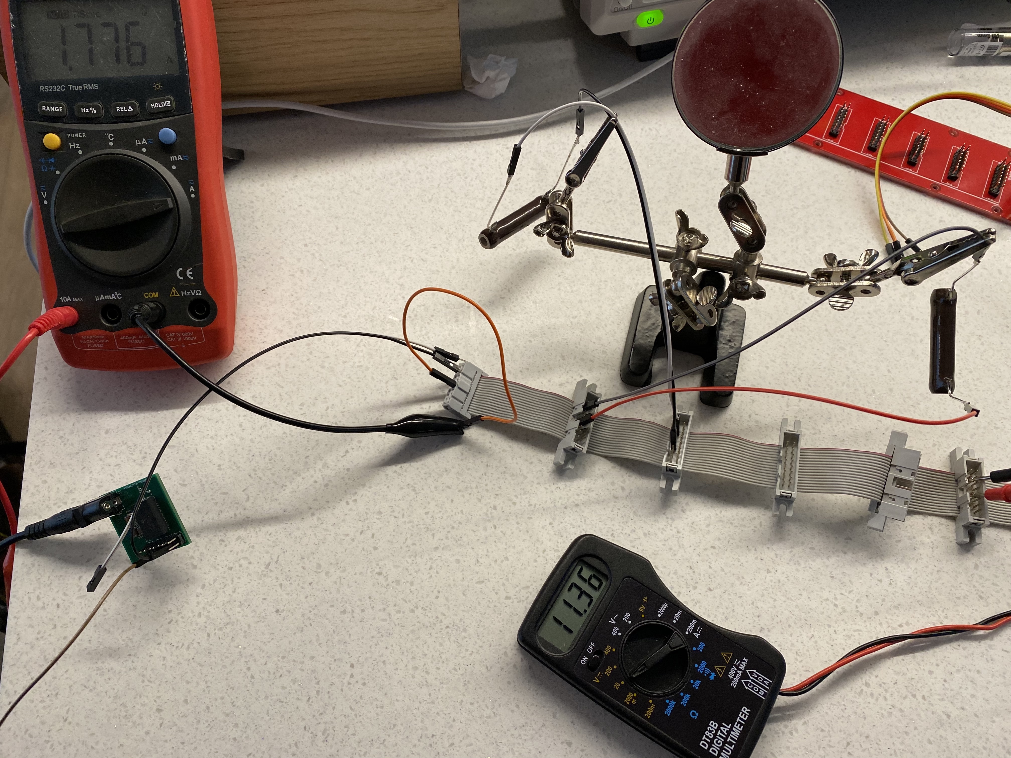
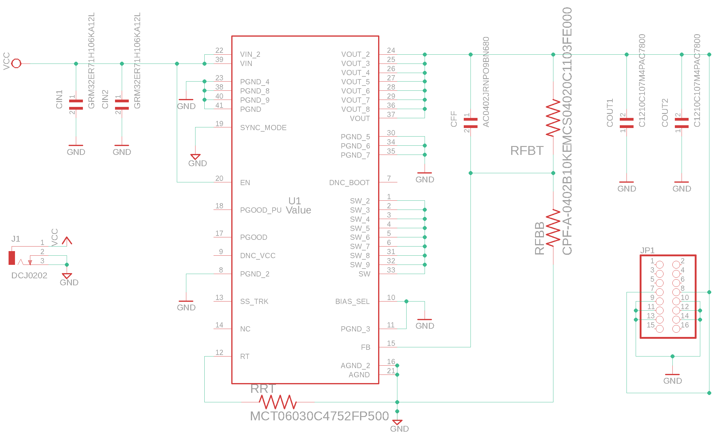
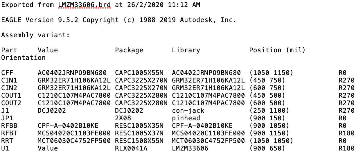
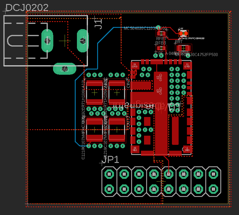
I have two 12 ohm resistors (rated 12w each) attached to a flying bus cable being powered by a board with the LMZM33606 chip.  The current being drawn is 1.776 A.  Using a multimeter to measure another port in the flying bus cable the voltage is only 11.36V and not the expected 12V.  Please advise what is the reason for this drop in voltage and how it can be fixed.  Thanks

  • FYI. The LMZM33606 board is being powered by a power adapter that supplies 15V 3A

  • It seems to me that the drop is from the additional resistance in the wires used to connect the two resistors.  Would that be the case here?

    Since Current = 1.776A, Volts is = 11.36 then the total resistance R = V / I = 11.36 / 1.776 = 6.3964 ohms - which is more than the 6 ohms total resistance for the two 12 ohm resistors in parallel.  

    Would using shorter and thicker wires to connect the two resistors bring the overall measured voltage of 11.36 V back up to 12 V?

  • Hi Spec Pro,

    If the load is far away from the device there can be an power drop across the wire (P=I^2R). One way to confirm this is by probing the voltage at the output pin or output capacitor(which I assumed in your PCB layout is close to the regulator) and compare it to the voltage you see at the load resistor. The closer the load is to the regulator the better since there will be less of a drop. 

    For testing purposes, can you directly solder the two 12ohm resistor directly to the output capacitor on your PCB and check output voltage regulation? This should eliminate the drop across the bus cable.

    Regards,

    Jimmy 

  • Dear Jimmy,

    Thanks for the suggestions on getting a better reading of the voltage drop.  I took two readings 1) across the output capacitor (2.709 Amps) and 2) at the load (2.703 Amps).  The results were as follows:

    1) At the output cap:

    Pk-Pk = 40mV

    RMS = 12.03V

    Min = 12.02V

    Max = 12.06V

    2) At the load (3 x 12ohm resistors)

    Pk-Pk = 216mV

    RMS = 12.03V

    Min = 11.92V

    Max = 12.14V

    Freq of waveform = 833.756 KHz

    The figures above were taken at startup.  When the regulator ran for almost two hours at the same load the Pk-Pk measured was around 140-160mV but would at times jump up to 200mV.  Please advise if these figures are as expected or if there's anything else I can test to make sure things are optimal.

    In my design, I have not separated the AGND from the GND will this affect the performance somehow?

    Cheers!

  • Can you confirm if the voltage at the output capacitance and load resistor is after removal of the bus ribbon cable as I suggested? From the voltage measurement it looks like the output voltage between Cout and load is around 12V typical. 

    If this is the case then it would indicate that the bus ribbon cable is causing the output voltage to droop from 12V at output capacitor to 11.36V at end of bus ribbon cable to load resistor in your original test measurement. 

    Can you provide the schematic and layout for me to review component selection? Output ripple that large would indicate that you are not using enough output capacitance. Please refer to Figure 16 which shows for a 24Vin/12Vout @ 500kHz, the output ripple should be around 15mV for a 4 x 47uF output capacitance.

    Regards,

    Jimmy 

  • Hi Jimmy,

    Yes the measurements were done with the bus cable removed and directly from the pins on the board.  Please find the schematics and BOM attached below for your reference.  Thanks and looking forward to any suggested changes to design or component selections.

  • I've received your schematic and am currently reviewing it. Will provide update by end of end of tomorrow.

    Regards,

    Jimmy 

  • In your schematic it looks like AGND and PGND are separate but from your previous reply "I have not separated the AGND from the GND" I'm assuming this is not the case.

     It is recommended to have AGND separate from PGND as stated in the datasheet. The power ground return (PGND) is a noisy plane.The goal of this separation is to create a low noise analog plane for components and loops that are sensitive to noise such as the feedback network and RT pin. This may be the reason why you are seeing high output ripple in your PCB.

    Another thing to consider is the input capacitor placement and the FB node. It is recommended to place the input capacitor as close as possible to the input pin to reduce stray inductance. This stray inductance and the discontinuous current that flows through it will result in noise generated on the output. Additionally, since the FB node is sensitive to noise, keeping the traces connection thin and top/bottom resistors close to the FB node will help minimize noise coupling which could cause high output ripple.

    Overall I think the first thing you want to do is keep AGND separate from PGND for noise isolation purposes. If that still is an issue, you may want to start looking into the input capacitor placement and minimizing the feedback network inductance. Lastly you can add additional output ceramic capacitors to help lower output ripple.

    Regards,

    Jimmy 

  • Hi Jimmy,

    Thanks for the detail feedback.  To keep the AGND separate from the PGND do I simply create another plane / polygon in Eagle cad and link up all the AGND to that plane?  Which layer of the board should that plane go on (top, upper middle, lower middle, bottom)?  

    Please find the board layout for the capacitor and feedback circuit (in blue) placements.  Kindly advise if the caps and resistors are close enough to their pins.  Is the blue feedback circuit in the right place?

  • Hi Spec Pro,

    You can put the AGND copper plane on the top layer similar to your PGND copper plane. Please look at Figure 48 in the datasheet for an example of the Top layer connection for AGND and PGND. The Rfbb resistor is right next to the FB pin and AGND pin with optimized current loop. The AGND has it's own dedicated polygon pour on both Top Layer for Rfbb and an entire bottom layer to have Rt connected. 

    The capacitor placement look similar to Figure 48 and the VOUT trace (blue) look similar to Figure 51.The resistor divider is close to the FB node and the inductance loop is minimized in your design. I think this looks fine. 

    Regards,

    Jimmy

  • Hi Jimmy,

    Thanks for the clarification.  Just to make sure I've understood correctly, please see the two diagrams below to see if I have outlined the AGND polygons correctly on the top and bottom layers.  When you refer to "Rt" do you mean the RT pin on the chip or the RT resistor?  Would also appreciate if you could let me know if the component selection is ok as well.  Many thanks!

  • Spec Pro,

    Yes you correctly highlighted the AGND on your first image. That image is to show how the AGND is separate from the PGND and is the only return path for sensitive circuits like the feedback resistor and Rt resistor. Also the second image shows the entire bottom layer is AGND as well.

    As for Rt, as long as you have Rt resistor connected to AGND it should be fine.

    Lastly, the component values you have look okay and shouldn't be a problem for operational stability of the device.

    Regards,

    Jimmy