This thread has been locked.

If you have a related question, please click the "Ask a related question" button in the top right corner. The newly created question will be automatically linked to this question.

LMG1210: Gate driver on the opposite side of the PCB of the GAN FET

Part Number: LMG1210

Hello,

We are designing a 150V three-phase inverter based on GAN FET and LMG1210. Switching frequency will be 100kHz. Due to space constraints, we cannot place gate driver and GAN FET in the same PCB side. 

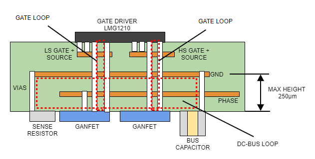
The current layout proposal places GAN FETs, current sense resistor and decoupling capacitors on the same side, while gate driver and bootstrap diode are on the opposite side. To minimize gate and source inductance, we will use multiple vias in parallel, with a maximum estimated inductance of 0.15 nH per via. See a diagram attached

Do you consider that this layout will cause many problems regarding ringings or oscillations?

Thank you for your help!

  • Hi Ricard,

    Thanks for reaching about on this for lmg1210. Im thinking this is for a motor drive application from the switching frequency.

    This layout diagram is ok and should not cause problems with ringing as long as the peak current through the GaN does not lift the ground voltage seen by the gate driver due to too much power or gate loop inductance. Since the driver is still a short distance away from the gate the inductance is minimized. To minimize common source inductance even more you can use vias-in-pad of the driver output pin and FET gate.

    Let me know if you have any other questions.

    Thanks,