This thread has been locked.

If you have a related question, please click the "Ask a related question" button in the top right corner. The newly created question will be automatically linked to this question.

TPS7A84A: schematic review

Part Number: TPS7A84A

Dear expert,

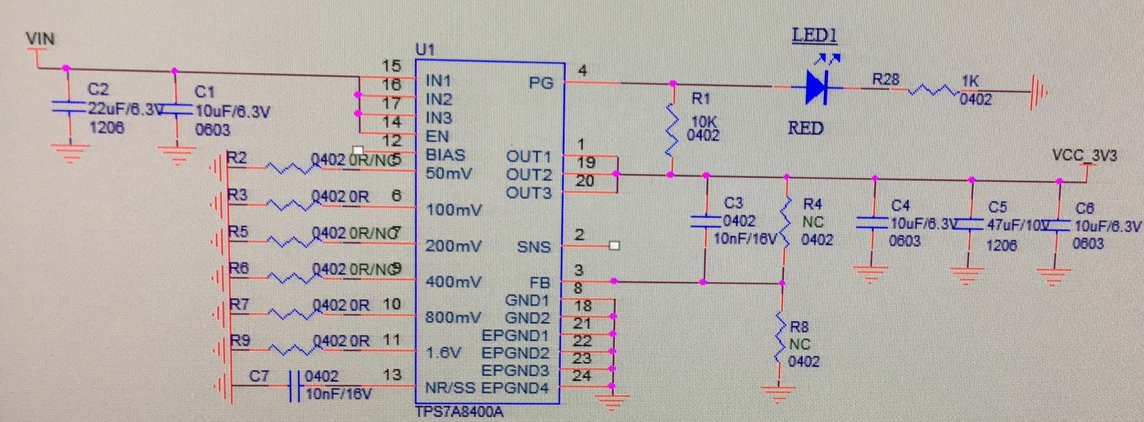
My customer is using TPS7A8400A to develop a low-noise, high-accuracy LDO, as shown in the figure. It is 3.3V ~ 5V input, 3.3V fixed voltage output, load current starts 2.5A, stable 0.9A. 

There are also several uncertain issues:
1. Does the SNS pin need to be connected to OUT without modifying the resolution of the internal reference voltage?
2. If the input and output voltage is greater than 2.2V, is it beneficial to reduce the noise by connecting bias to the power supply pin?
3. Can the PG pin be connected to the LED light to indicate whether the circuit is faulty? Is there a problem if I connect as shown in this picture?
4. How to judge which one is used, the internal fixed voltage or the resistance voltage division on the FB pin?
5. In order to achieve the best effect of suppressing noise and high frequency, are there any improvement of the input and output filter capacitors and other bypass capacitors as shown in the figure?

Thanks for your support!

  • Hi Mingqi,

    The answer you questions:

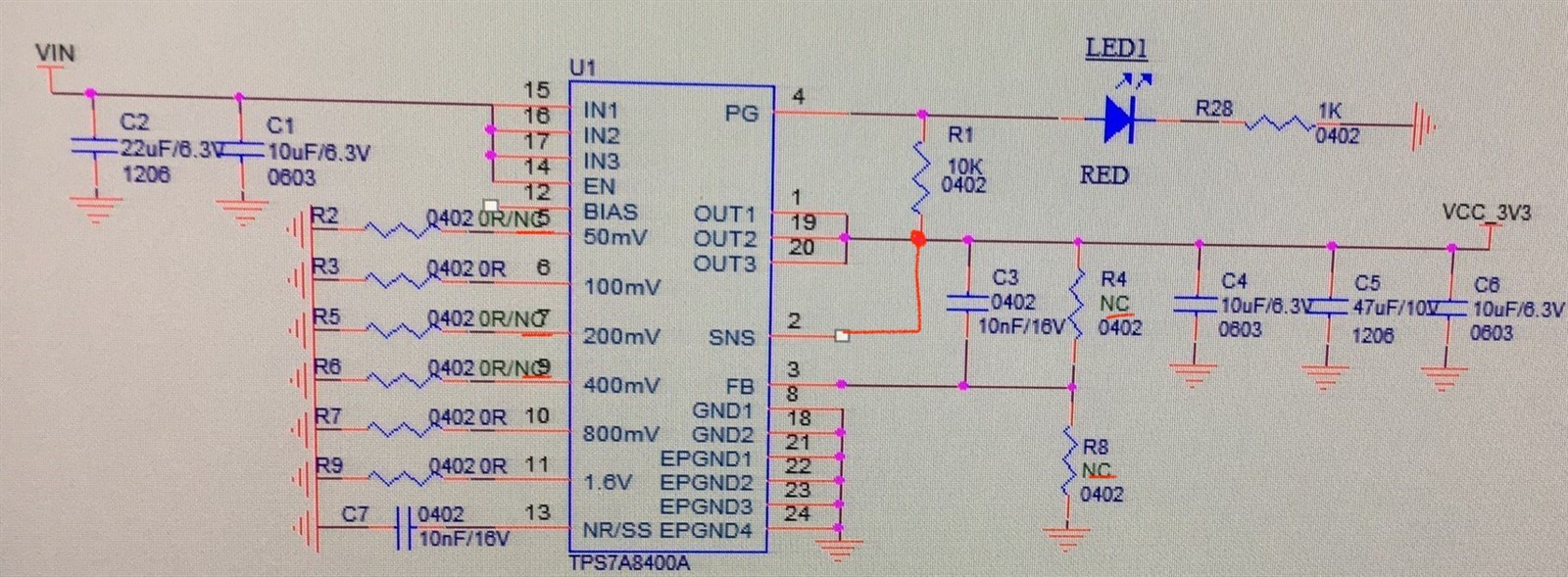
    1. Does the SNS pin need to be connected to OUT without modifying the resolution of the internal reference voltage? *If R4 and R8 are not populated and the Any-Out feature is being used, SNS must be tied to VCC_3V3. 
    2. If the input and output voltage is greater than 2.2V, is it beneficial to reduce the noise by connecting bias to the power supply pin?*Connecting VBIAS to a higher voltage can help with PSRR. The internal charge pump doubles VIN but has a clamp at 6.5V. If VIN is 5V, there is no measurable difference. 
    3. Can the PG pin be connected to the LED light to indicate whether the circuit is faulty? Is there a problem if I connect as shown in this picture? *The PG pin is an open-drain output. As long as the LED has enough voltage and current this will work. 
    4. How to judge which one is used, the internal fixed voltage or the resistance voltage division on the FB pin? *The advantage of using Any_Out is that you don't have to consider the impact of the feedback resistors on accuracy. Also, this simplifies the BOM as one of the feedback resistors is likely a unique value on the board. The disadvantage is that the step size is 50mV. With FB resistors, you have much finer control over VOUT but the thermal noise of the resistors (while minor) is added to the overall noise. 
    5. In order to achieve the best effect of suppressing noise and high frequency, are there any improvement of the input and output filter capacitors and other bypass capacitors as shown in the figure?* Schematically after the SNS connection is made (maybe using a 0-Ohm resistor), This looks OK. The only other area which can impact noise and PSRR performance is in the layout. See our LDO basics series for more details. 

    I hope this helps to clarify.