This thread has been locked.

If you have a related question, please click the "Ask a related question" button in the top right corner. The newly created question will be automatically linked to this question.

TPS65023: Ramp up time of LDOs

Part Number: TPS65023
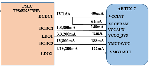
Other Parts Discussed in Thread: , TPS650250, TIDA-050000

Hi,

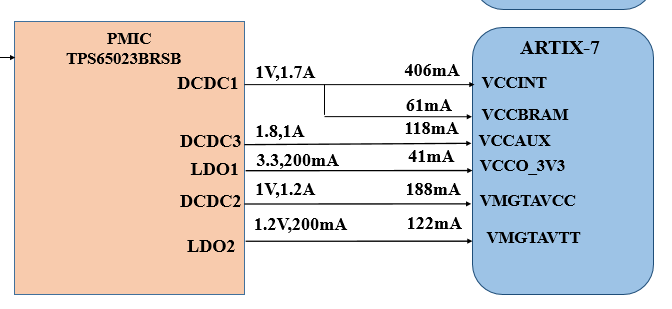
I am using TPS65023 my design power ARTIX-7 FPGA XC7A50T-2CPG236C. What s the ramp up time of LDO 2 and 3.

  • Shifali,

    Can you share a schematic or block diagram showing your mapping of PMIC output rails to the FPGA? I am wondering which of the Artix-7 rails are being supplied by LDO1 and LDO2. LDO1 = pin 20, LDO2 = pin18, VINLDO = pin 19, and LDO_EN = pin 22 which enables both LDO1 and LDO2 at the same time. There is a 3rd LDO, VRTC, which only supplies 30mA and I do not think it would be used to power Artix-7.

    Are you concerned that the ramp time of the LDOs will be too fast, or are you concerned that it will be too slow?

    For the DCDCx regulators, the ramp time (tRamp) is specified with a typical value of 750us after a delay from EN high to start switching (tStart) with a typical value of 175us. This is because the DC-DC switching regulators have soft-start and take longer to ramp up to the target value.

    You can see when comparing Figure 22. Start-Up VDCDC1, VDCDC2, and VDCDC3 and Figure 23. Start-Up LDO1 and LDO2 in the TPS65023 datasheet that the LDOx ramp times are much faster than the DCDCx regulators.

    LDO1 and LDO2 total ramp time is approximately 120-140us depending on the output voltage of the LDO.

    The LDO slew rate appears to be controlled and constant at 500mV/50us = 10mV/us, which is clearly visible in Figure 23.

  • Hi Brian,

    Please find the attached block diagram.

    And yes I will be using LDO1 and LDO2.

  • The output voltage of LDO1 and LDO2 is determined by the DEFLDO1 and DEFLDO2 pins:

    DEFLDO2 DEFLDO1 VLDO1 VLDO2
    0 0 1.3 V 3.3 V
    0 1 2.8 V 3.3 V
    1 0 1.3 V 1.8 V
    1 1 1.8 V 3.3 V

    As a result, TPS65023B will never generate 3.3V on LDO1. The best option is DEFLDO2=0 & DEFLDO1=0 (both shorted to GND), but this means your block diagram has LDO1 and LDO2 backwards. In this case, VLDO2 = 3.3V and VLDO1 = 1.3V, but VMGTAVTT requires a 1.2V supply. The only way to generate exactly 1.2V would be to apply power to the PMIC, keep LDO_EN = Low initially so you can write I2C to LDO_CTRL (Register 0x08) to change the output voltage to 1.2V before enabling the LDOs.

    Based on your power tree, may I recommend using the TPS650250 instead. This would be the best wiring:

    • DCDC1 = 1.0V, 1.6A for VCCINT (same as your diagram)
    • DCDC2 = 3.3V, 800mA for VCCO
    • DCDC3 = 1.8V, 800mA for VCCAUX (same as your diagram)
    • LDO1 = 1.0V, 200mA for VMGTAVCC (power supplied from DCDC2 or DCDC3 to improve efficiency)
    • LDO2 = 1.2V, 200mA for VMGTAVTT (same as your diagram, but power supplied from DCDC2 or DCDC3 to improve efficiency)

    TPS650250 will allow you to set the output voltage of every rail with external resistor divider, even for LDOs. Based on your power tree, the TPS650250 can supply the amount of current required by each rail of the Artix-7 in this design.

  • Hi brian,

    Thank you for suggesting an alternate PMIC. Attached is the  configuration of new PMIC and ARTIX-7. Just reconfirm it. Also what is the ramp up time of LDos. Is it 140us.  

  • The block diagram you have re-drawn does not match my recommendation. My recommendation is below:

    • DCDC1 = 1.0V, 1.6A for VCCINT (same as your diagram)
    • DCDC2 = 1.8V, 800mA for VCCAUX  (same as your diagram)
    • DCDC3 = 3.3V, 800mA for VCCO_3V3 (not the same as your diagram)
    • LDO1 = 1.0V, 200mA for VMGTAVCC (not the same as your diagram)
    • LDO2 = 1.2V, 200mA for VMGTAVTT (same as your diagram)

    If you swap DCDC3 and LDO1, your diagram will match my recommendation.

    It is best to power both MGTAVCC and MGTAVTT rails from LDOs, because it will be cleaner supply (no switching noise).

    LDO Ramp Times

    The LDOs in the TPS650250 turn on with an uncontrolled ramp from 0V to 0.75V (this is fast, approximately 40us), then they ramp at a constant slew rate of approximately 3 mV/us.

    For LDO1, set to 1.0V in my recommendation, I expect the total ramp time to be 40us + (3.3-0.75)V/(.003V/us) = 123us

    For LDO2, set to 1.2V in your design, I expect the total ramp time to be 40us + (1.2-0.75)V/(.003V/us) = 190us

  • Hi Brian,

    The rail VMGTAVCC consumes 188mA as per our estimation. This current may vary. The maximum current from LDO1 is 200mA. Hence to aviod the border condition i have connected it to DCDC3 and VCC0_3V3 to LDO1 since it just consumes 41mA. 

    I hope this configuration will also work. please confirm.

  • Your proposal to use DCDC3 to provide 1.0V will probably work, but you may need to add a lot of bulk capacitance to ensure that the ripple voltage does not exceed +/-10mV as is recommended by Xilinx for VMGTAVxx rails.

    However, my recommendation was that DCDC3 = 3.3V and can also supply input voltage to LDO1 and LDO2, if the sequencing of Artix-7 will allow this.

    So instead of 41mA load for DCDC3, you would have 41mA + 188mA + 122mA = 351mA and the power loss in the LDOs would be reduced.

    The short-circuit protection for the LDOs in TPS650250 is set to 400mA, so I do not think you risk over-loading the LDO at 188mA. 200mA is the continuous output current that it is rated for across voltage and temperature conditions.

  • Hi Brian,

    I have another concern. The DCDC1 regulator rail is 1V. Since to follow power sequence I planned to enable DCDC2 from output of DCDC1. But En pin VIH is 1.45. Hence i cant enable like that. Can i add RC circuit for delay to EN_DCDC2 pin so that i can maintain sequence. Or is there any other way so that i can maintain power sequence.

  • You can use PWRFAIL_SNS comparator to detect when DCDC1 > 1.0V and PWRFAILz output to enable DCDC2.

    The trick here would be to set VDCDC1 = 1.03V nominal so that the comparator is guaranteed to detect VDCDC1 > VREF = 1.0V +/- 2% = 1.02V max to detect a rising edge. The hysteresis will prevent it from detect a falling edge until VDCDC1 < VREF - Vhys.

    This will allow you to enable DCDC2 from DCDC1 valid output voltage.

  • Hi,

    Can you please share any reference schematics of TPS650250 for XILLINX-7 series FPGAs.

  • Shifali,

    You can refer to TIDA-050000 for reference schematics using TPS65023 for Xilinx 7-Series devices. TPS650250 schematic would be very similar.

    However, your block diagram is different than the block diagram we proposed in TIDA-050000 because the power requirements from your XPE file are much lower than the estimates for the entire Artix-7, Spartan-7, and Zynq-7000 families that we designed for initially.

    Either way, TIDA-050000 is a good starting point and you can start a new e2e thread if you have any follow-up questions on your design.