This thread has been locked.

If you have a related question, please click the "Ask a related question" button in the top right corner. The newly created question will be automatically linked to this question.

DSG Drive abnormal shutdown

Part Number: BQ76930

Hi:

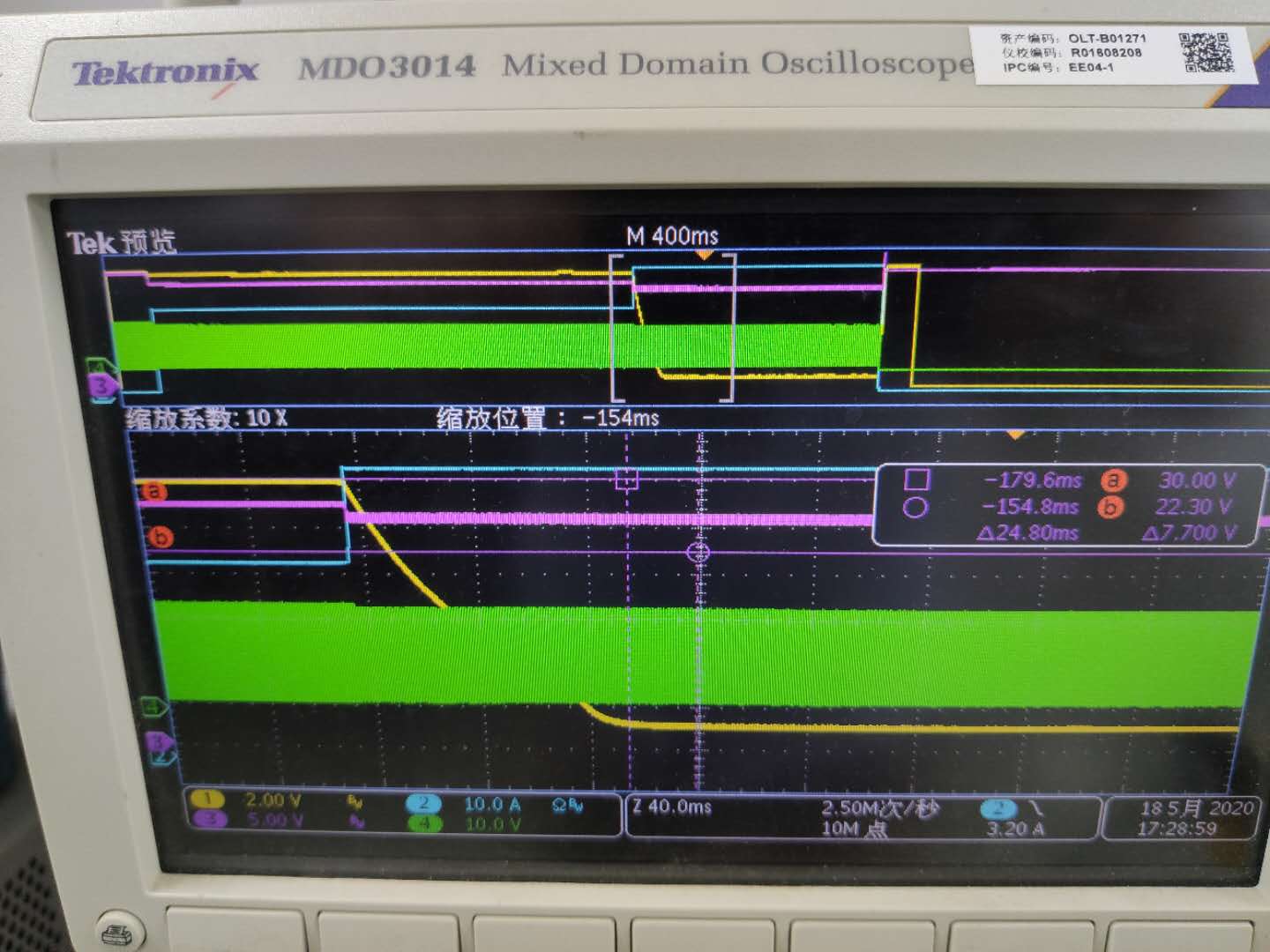
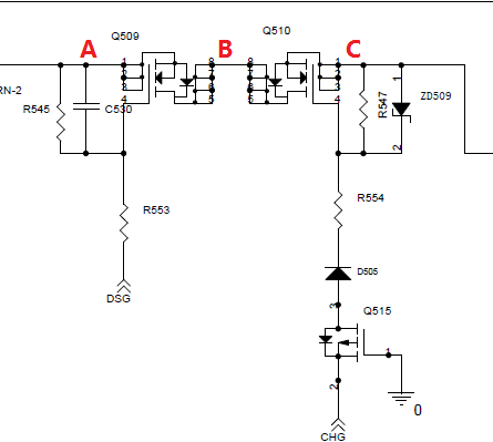
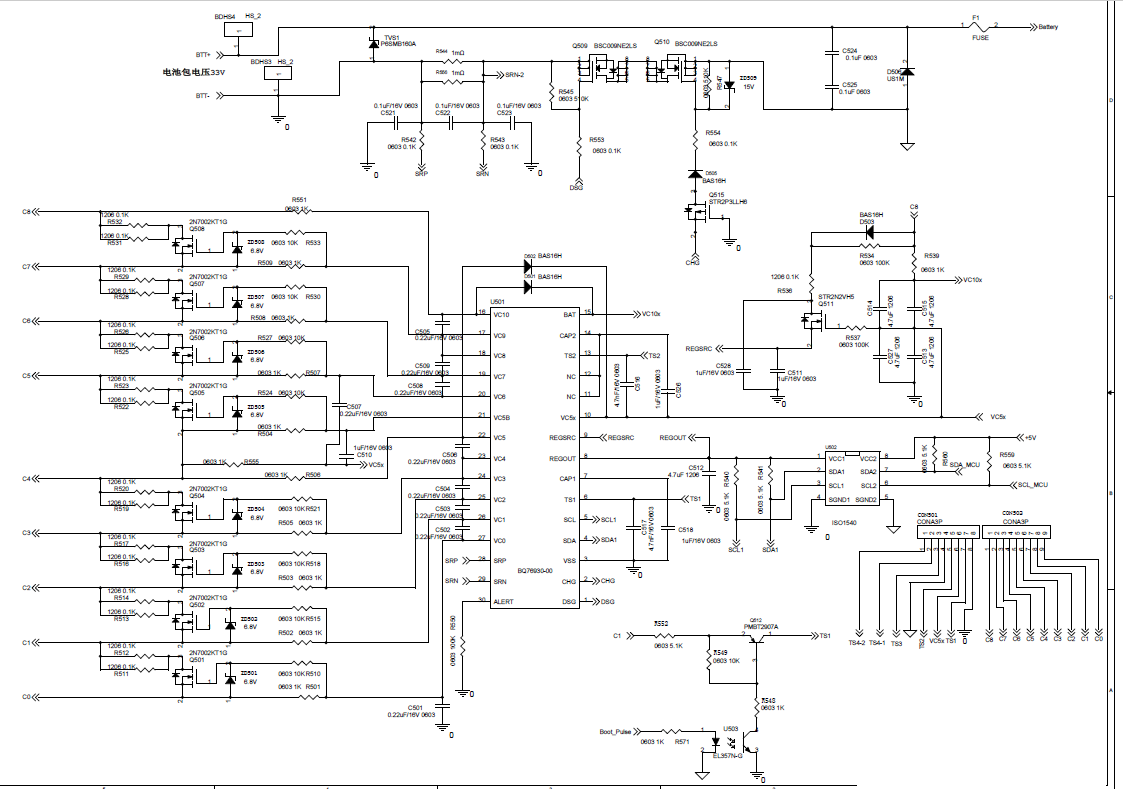
I am use Bq76960 to manage a 8S1P battery pack(sony 18650 vtc6);when i increase the load to 800W,the DSG driver will slowly go low,continue about 100ms-120ms(there is a 220nF SMD cap at the Discharge MOSFET G-S),it seemed that the chip DSG PIN has no sink capability;At normal shutdown situation,DSG will fall in no more then 10ms,that is OK;

Below is the Picture:(Note:I'v short the Charge MOSFET D-S;)

CH1:DSG               CH2:Discharge Buck Output(12V) Current        CH3:Battery Voltage     CH4:Discharge Buck SW Voltage

  • Hi User,

    You do not describe the connection of the DSG to the FET other than the capacitor.  With 220 nF and the internal 2.5k ohm the time constant would be about 550 us if there were no resistance between DSG and the gate, and if aRgs resistor was not used. Since turn off without the switching load is better, it may be that the DSG drive voltage goes low slowly due to loss of power.  Check the REGSRC voltage during the event to see if it is dropping off.  If it drops determine how the switching regulator depletes the REGSRC supply. 

    If the problem is not apparent after testing the supply voltage, a schematic section may be helpful.

  • Hi:

    I'v retested the circuit;Below is my circuit and test result;For Debug Purpose,R553,Q509,Q510 has been removed;Wire A and B,C has been connect together;The Chip DSG PIN fall in 8.5ms(Normal fall time is ~5us);  The REGSRC voltage is about 12.9V~14V;

    CH1:DSG PIN        CH2:REGSRC PIN      CH3:Bat Voltage     CH4:Discharge Buck SW Voltage

  • Hi User,

    That is certainly curious.  The increased load seems to upset something for the part.  It would not seem to be REGSRC from the capture.With the heavier load is something being driven below VSS? 

    Is there a fault indicated?  I presume not since you indicate the pin can switch promptly and in the first picture DSG seems to come back as soon as the load is released.

    The FETs are bypassed, is CHG still connected and ON during the test?  What is its waveform?

  • hi,

         i'v tested more pin voltage of the chip;no voltage below vss;CHG falls too just like DSG,~8.5ms

  •  here is the test graphic:

    CH1:DSG          CH2:CHG         CH3:BAT VOLTAGE

  • Hi User,

    That is interesting.  The power supplies into the chip appear stable but the characteristic signal from the load is disrupting the FET output voltage in a non-distructive manner. I don't recognize if you have used a common schematic, if the part indicates any fault, or if it communicates with the MCU during this situation.

    You might try another part to be certain it is not a damaged device, otherwise you will need to determine how the interference is getting into the part and eliminate the path with improved connection or filtering.

  • Hi

         this is my schematic,I'v tried to break the communicate with MCU,and tried a new part,the issue still occured ,please check my application schematic,tks!

  • Hi User,

    The schematic does look quite normal.  The isolator in the communication path should normally prevent issues with the MCU communication and the low side switch.  The only things which look odd:

    The bottom of C502 for VC1 should connect to VSS as shown in the data sheet.  Connecting as you have done can cause VC0 to be pushed below VSS, is not known to cause a problem, but perhaps if your dynamic load could be causing the issue.

    The REGOUT, SCL1, SDA1 have off page symbols, not sure if they are going to something which brings a signal into the IC. 

    You might look for paths which couple onto the IC pins or isolate signals until the issue goes away.