This thread has been locked.

If you have a related question, please click the "Ask a related question" button in the top right corner. The newly created question will be automatically linked to this question.

TPS650864: GPO2 in Power map example

Guru 16770 points
Part Number: TPS650864
Other Parts Discussed in Thread: TPS51200

Hi

I'm referring datasheet of TPS650864, whose version is SWCS138C, and I have a question for Figure 6-3 TPS6508640 Power Map example.

It was not clear for me how to use GPO2 in Figure 6-3.

Could you tell me a role of GPO2 as I2C GPO in Figure 6-3.

BestRegards

  • Hello,

    GPO2 has no role in the system. It is just an open drain general purpose output that can be open or short to GND by GPO2_LVL bit. Generally it is not used unless your SoC runs out of pins and you could use an extra GPO from the PMIC.

  • Hi Kevin

    Thank you for your reply.

    >GPO2 has no role in the system. 

    I looked into SWCC027.ZIP to see the settings of TPS6508640.

    In sequence tab, a cell with GPO2 crossing BUCK6_PG is Yes.

    I think it means GPO2 works as BUCK6 Power-Good.  Is my understanding wrong?
    (With the same iidea, I believe GPO1 should offer BUCK2 Power-Good function.)

    BestRegards

  • Hi,

    You are correct for GPO1.

    For GPO2, the GPO2 PG circuit is being used to enable the VTT LDO but it is not connected to the GPO2 pin. You can see this on row 47 of the Overview sheet. The logic is shown as the second image on the Sequencing tab.

  • Hi Kevin

    Thank you for your reply.

    Let me confirm the condition of VTT LDO to be enabled.

    On the row 84 (GPO2) of the sequencing sheet, crossing cell with BUCK6_PG, CTL3, CTL4 and CTL5 is filled by "yes".

    I thought VTT LDO would be enabled automatically in result of asserting CTL3&CTL4&CTL5&BUCK6_PG.  Is it correct?
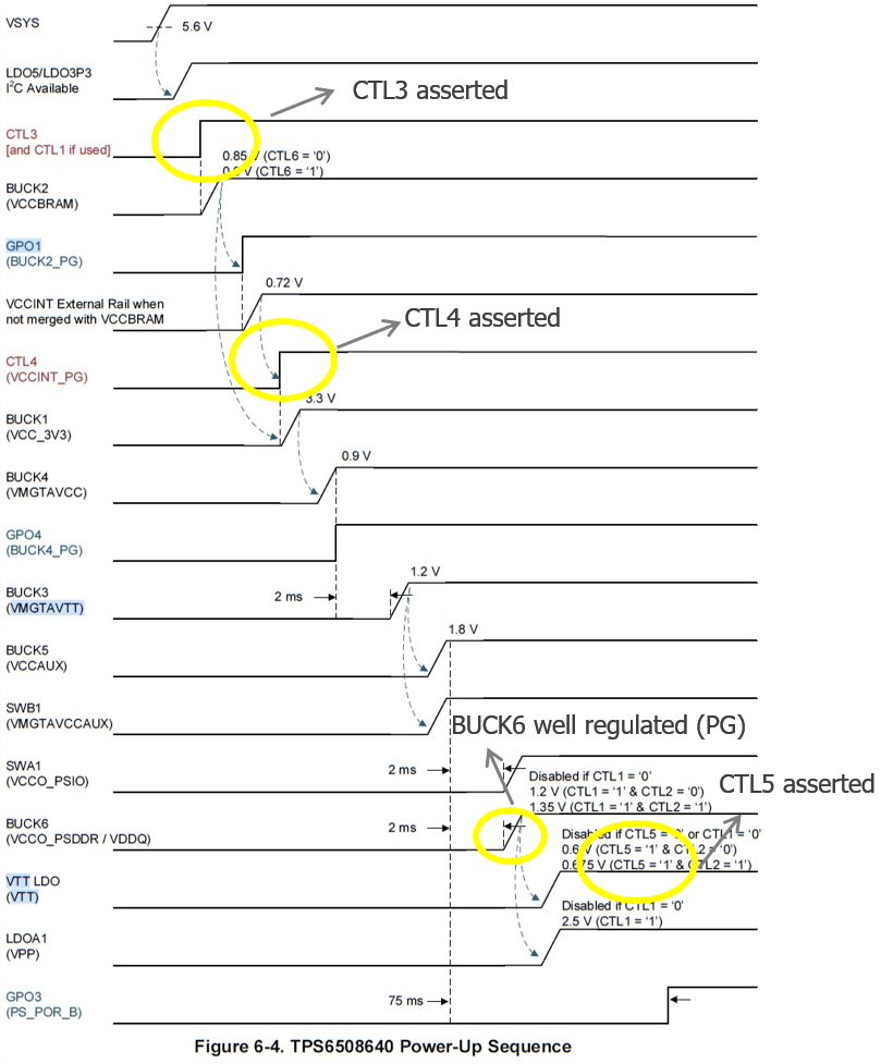
    Actually, TPS6508640 power up sequence looks like as so.

    BestRegards

  • Hello,

    You are correct that VTT LDO enable is essentially an AND gate with the CTL3&CTL4&CTL5&BUCK6_PG as inputs. 

    Typically this means that you can tie CTL5 to LDO3P3 if you want to have VTT enabled after BUCK6_PG or you can tie it to GND if you don't need to use VTT LDO. This will depend on what type of DDR you are using or if you prefer to use TPS51200 for example. LPDDR4 for example does not need termination.

  • Hi Kelvin

    Thank you for your reply.  I understand.

    I will use BUCK6 with 1.2V settings for VDDQ of DDR4.
    So VTT LDO will be set to output 0.6V.

    I will connect CTL5 to LDO3p3 following your advice.

    By the way, I have just wondered where CTL3 and CTL1 to be connected.
    I want to enable BUCK6 after BUCK5, and LDOA1 being enabled after BUCK6.
    So, I connect CTL3 and CTL1 together as mentioned in the datasheet.

    Page 26,
    "Connecting the CTL1 pin to the same input as CTL3 will result in BUCK6 being enabled 2 ms after BUCK5 and LDOA1 being enabled after BUCK6 PG. "

    In addition, I will connect them to LDO3V3.  As a result, CTL3, CTL1 and CTL5 will be connected to LDO3p3.

    Is it capable? 

    LDO3p3 can output 30mA as maximum, so I think it would be OK..

    BestRegards

  • Hi,

    They are high impedance inputs so power draw from LDO3P3 is minimal. The system to be always-on with no way of shutting off when CTL3 is connected to LDO3P3. In case of any faults, the PMIC will perform an emergency shutdown, reload the NVM memory, and attempt the power up sequence again (since CTL3 is always high).

  • Hi Kevin

    Thank you for your reply.

    >The system to be always-on with no way of shutting off when CTL3 is connected to LDO3P3.

    Can I consider CTL3 is an enable pin to start sequence followed BUCK2?

    BestRegards

  • Yes, CTL3 is acting as the enable pin and BUCK2 will be the first rail enabled, followed by GPO1. Remainder of sequence will execute once CTL4 goes high. 

  • Hi Kevin

    Thank you for your reply.

    I understand.

    BestRegards