This thread has been locked.

If you have a related question, please click the "Ask a related question" button in the top right corner. The newly created question will be automatically linked to this question.

TPS74401: VBIAS vs performance

Part Number: TPS74401
Other Parts Discussed in Thread: TPS7A84A

Hello,


Datasheet 8.2.1.2 says as follows.


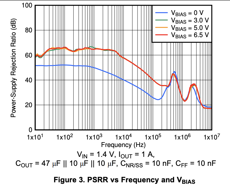
VBIAS = VOUT + 1.62 V = 3.12 V; the system has a 3.3-V rail to use for this supply and also to provide some limited headroom for VBIAS. The 5-V rail is a better choice to improve the performance of the LDO, so the 5-V rail is used.


Though datasheet specifies VBIAS must be more than Vout + 1.62V, it also recommends much more than Vout + 1.62V to improve the performance. But what does the performance mean here?

When VBIAS = 3.12V what performance is actually degraded, and how much?

When VBIAS = 5V what performance is actually improved, and how much?


Best regards,


K.Hirano

  • HI Hirano-san,

    The VBIAS rail is used to provide the headroom for the N-Channel FET used to regulate VOUT. See the charts below:

    When VOUT is below 1.62V, the drop-out increases quickly. so it becomes difficult to maintain regulation. 

    For 3.3V rail, having VBIAS at 5V, 5V-1.62V is 3.38V which is the maximum recommended regulation voltage. This does not have much margin.

    We have newer devices like the TPS7A84A which has an internal charge pump and the use of the VBIAS rail is optional.

    Does this help to clarify?


  • John,

    Thank you for your response.


    But, I am sorry, I do not still understand well why datasheet recommends VBIAS=5V instead of VBIAS=3.3V.

    The reason is just to have better margin against Vout + 1.62V = 3.12V?

    So datasheet is just mentioning (5V – 3.12V) = 1.88V margin is better than (3.3V – 3.12V) = 0.18V margin?

    No other performance differences at all?


    Best regards,


    K.Hirano

  • HI Hirano-san,

    If VBIAS is 3.3V, then the maximum regulation voltage would be 1.68V. This maximum voltage regulation voltage is in drop-out. Meaning the LDO has essentially no PSRR and likely would not respond well to a load transient. 


    If your load is regulating 1.2V or 1.5V this is probably OK, but PSRR is impacted.  Unfortunately, the TPS744 datasheet does not have a plot showing PSRR over VBIAS, but the TPS7A84A does:

    You can imagine if VBIAS is slowly lowered from 3V to 0V, you would see the PSRR degrade proportionally.

    Please note; the reason VBIAS can be 0 here is that this device has an internal charge pump. This takes VIN and doubles it to create its own internal VBIAS rail or it simply uses the external VBIAS rail if supplied. The TPS744 does not have an internal charge pump so it must have an external VBIAS applied. 

    Does this help to clarify?