This thread has been locked.

If you have a related question, please click the "Ask a related question" button in the top right corner. The newly created question will be automatically linked to this question.

TPS54225: TPS54425 OCP & latch issue

Part Number: TPS54225

HI SIR

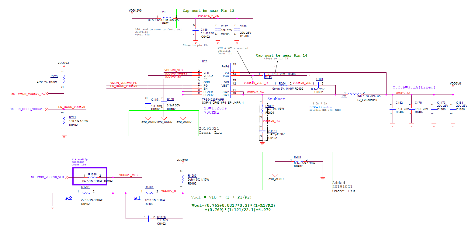
We use tps54225 to design 12v to 5.0V power supply, two problems are as follows
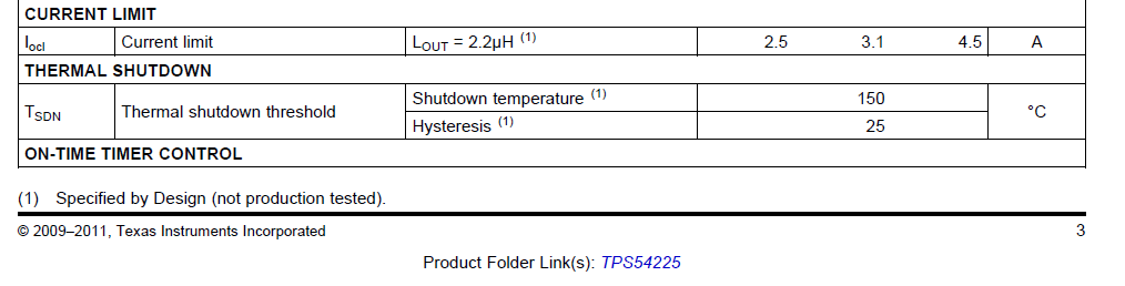
1. Is the OCP current limiting condition a valley current or a peak current?
2. When the OCP starts to enter the UVP, the IC enters the shutdown state, the enable continues to provide 3.3V,
    but the IC does not automatically restart to output 5.0V. We must turn off 12V and provide 12V again, ic can restart. Is this latch an IC feature?

Mick_Kao@alphanetworks.com

  • Hello Mick,

    • Yes, the Over current protection of the TPS54225 is using a cycle-by-cycle valley detect control circuit.
    • When the over current condition is removed, the output voltage will return to the regulated value. This protection is non-latching. BUT this at condition that the UVP is not triggered. Based on you wave form the UVP is triggered, the UVP protection is latching, you have to cycle EN to recover from it.


    Thanks

    Tahar

  • Hi Tahar

    As shown in the figure below, the ocp inductor current waveform min value is about 1.88A.
    Although the cycle by cycle OCP condition of reducing duty has begun to appear, it has not reached the velley trigger value (min 2.5A).
    Which condition should I pay attention to?
  • Hi, 

    The Load Current should not be more the 1/2 Ipp+minIL. In your case it will be around 2.5A. 

    Thanks! 

    Tahar

  • Hi Mick,

    The reason for that, the TPS54225 is PWM controlled, the Low peak can be detected but the limit will not take effect until the next switching cycle. if the switching cycle and the peak detection are aligned, you will see the low pick right at the OCP limit.  

     Thank!

    Tahar

  • Hi Tahar

    We find the reason for early protection.
    Because PGND is not directly connected to the common GND of the input and output, the inductance return path of the low side mosfet is too long and too thin, which causes the ic function to be abnormal.
    It has been resolved, thank you for your previous comments.