Hi experts,
I'm designing a VSI using GaN switches. My question lies in the PCB layout. As stated in EPC and GaN Systems white papers, the best layout practice is to use a 4 layer board, use top layer for VDC+ and mid-layer1 for PGND. This way the power loop spans over the top and mid-layer1 only. As the distance between the 2 layers is 8mils, there will be strong self-field cancellation which will reduce the loop inductance significantly compared to conventional lateral and vertical loops.
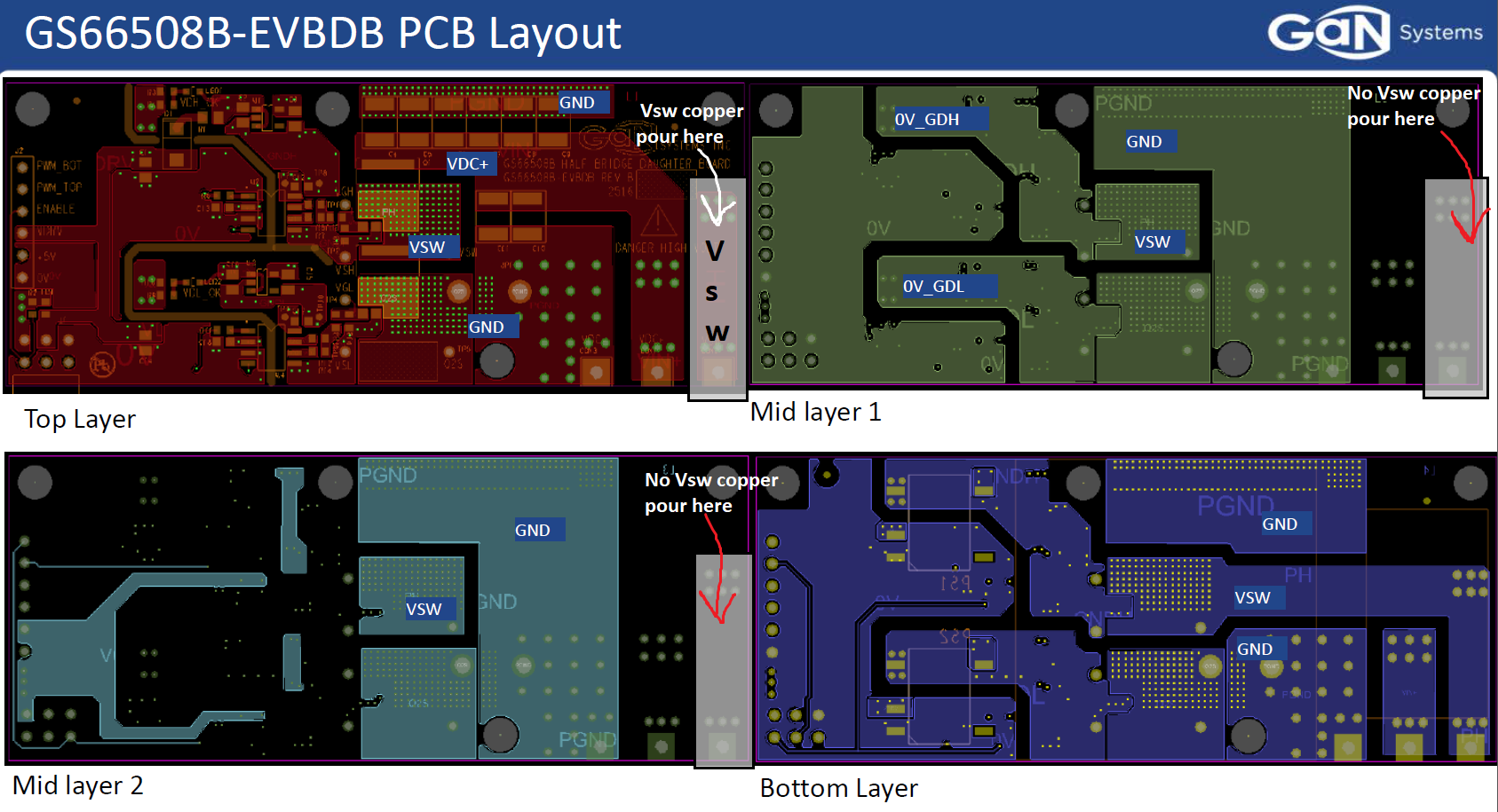
However, I came across a GaN Systems design which seemed rather odd. Here is the 4-layer design. I'm highlighting the gan switches as yellow boxes
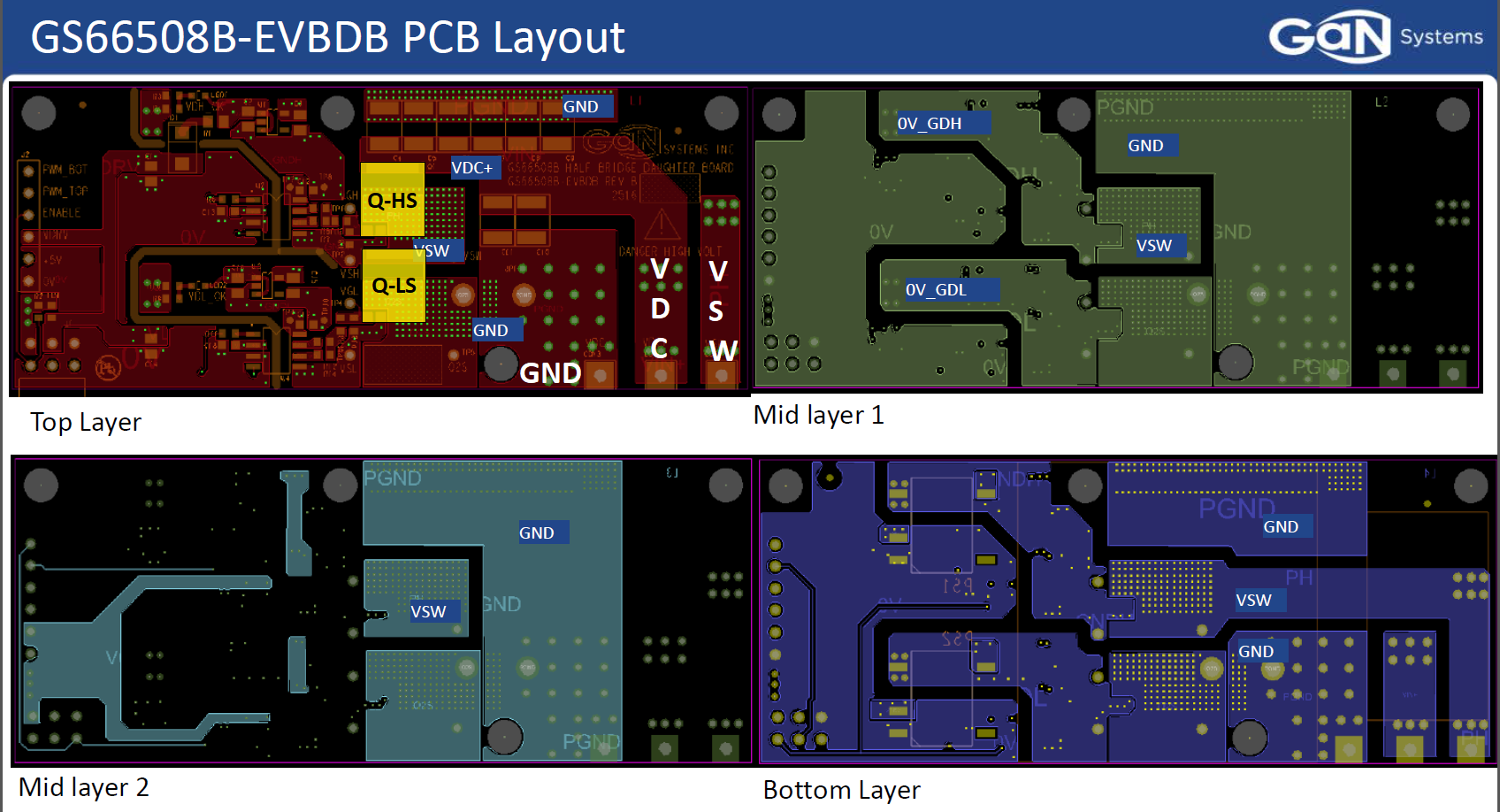
This design uses top layer for VDC+. Mid-layer 1 is used as PGND. But along with that, mid-layer 2 is also used as PGND. Also, there are 2 DC-Link capacitors on the top layer which make up a lateral power loop. So this means, this design uses 3 power loops in parallel (top-top lateral, top-mid1 vertical and top-mid2 vertical)
I'm attaching a picture to highlight the 3 power loops

WHITE ->Top-Top lateral Loop
BLUE -> Top-Mid1 vertical loop
PINK ->Top-Mid2 vertical loop
Since the 3 loops will have different inductances L1,L2,L3, the effective power loop inductance Lp will be L1 || L2 || L3. This means that inductance Lp will be lower than the smallest of L1,L2,L3.
But if observed from a flux point of view, this seems counter-intuitive. All the 3 loops will produce flux which will add up 'constructively' and as a result the effective power loop will possess flux greater than that produced by the least inductance loop (top-mid1). Thus, from a flux point of view, Lp will be greater than the smallest of L1,L2,L3
What is happening here? Why are multiple gnd return paths being used in this design? Is it good to use multiple return paths for a power loop?(ignoring the reduced resistance which paralleled paths offer).
Also, the traces Vsw and VDC are extended only on top and bottom layers. They could have put VDC and Vsw pours on mid-layer1 and mid-layer2 but they didnt. Why?