This thread has been locked.

If you have a related question, please click the "Ask a related question" button in the top right corner. The newly created question will be automatically linked to this question.

LM5035: Two abnormal phenomena during the startup and shutdown of half-bridge power supply based on LM5035

Part Number: LM5035
Other Parts Discussed in Thread: LM5110

Hello seniors,
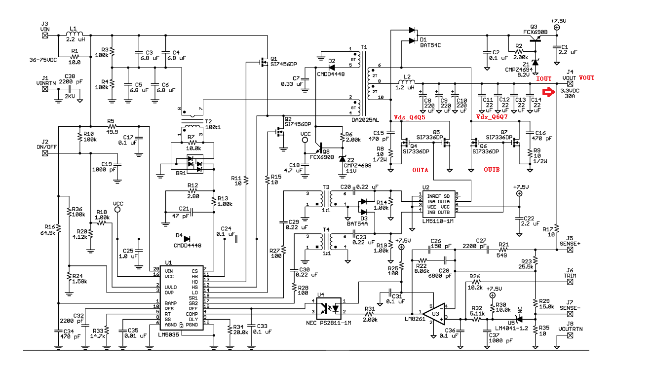
I modeled the 48V to 5V prototype based on the half-bridge circuit in the LM5035 manual. The circuit diagram is similar to the following figure:

During commissioning, it is found that there is one abnormal phenomenon in the secondary synchronous rectification part at the moment of starting and shutting down. Please also give pointers.
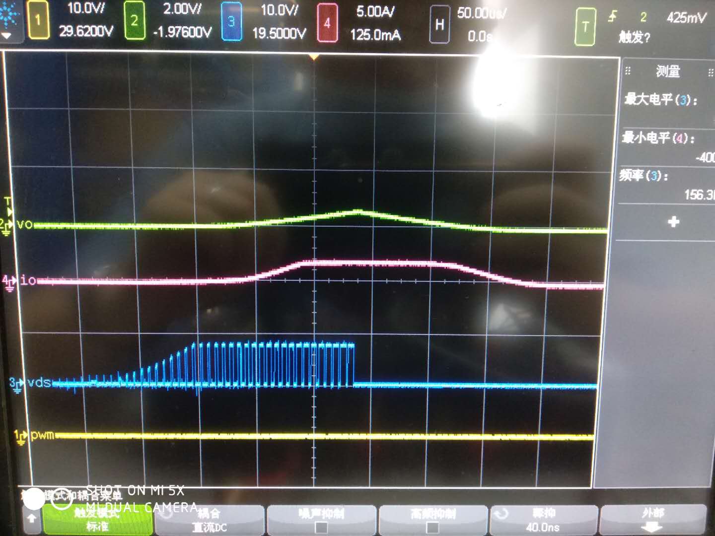
During startup, the output waveforms of OUTA and OUTB of the secondary synchronous rectifier driver U2 are different, as shown below:

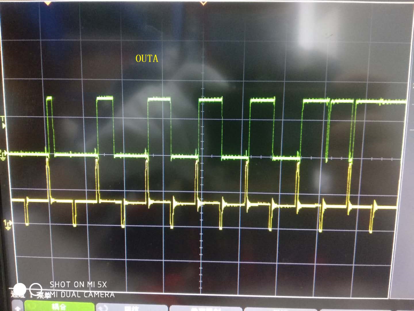
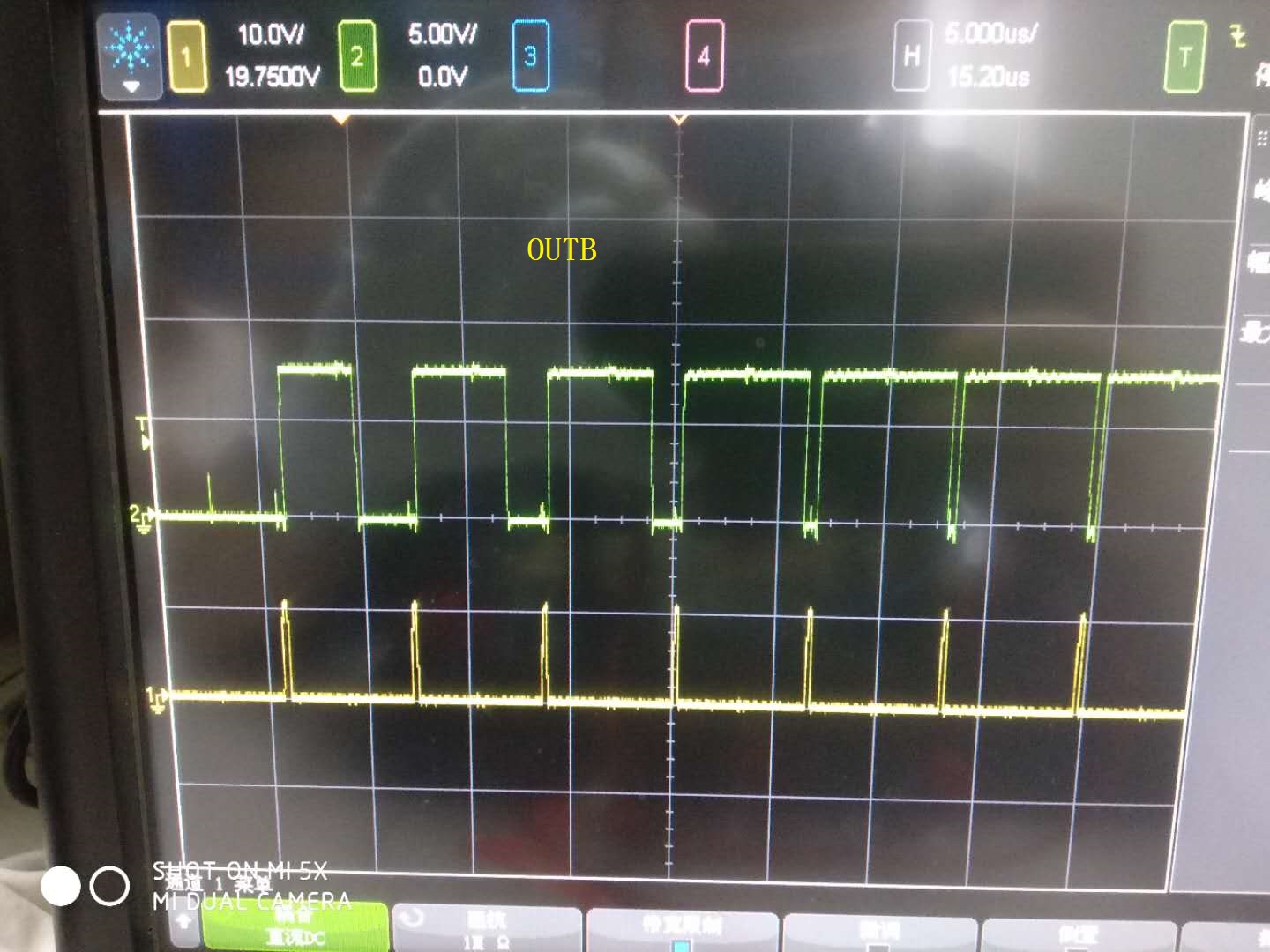
As shown in the above two figures, OUTB gradually increases at the instant of no-load startup, and about 4 cycles are stable, while OUTA requires 6-7 cycles, and the shapes of the two are inconsistent. The yellow-colored PWM wave is the corresponding primary MOS tube driving wave.
Not sure why OUTA and OUTB are inconsistent?

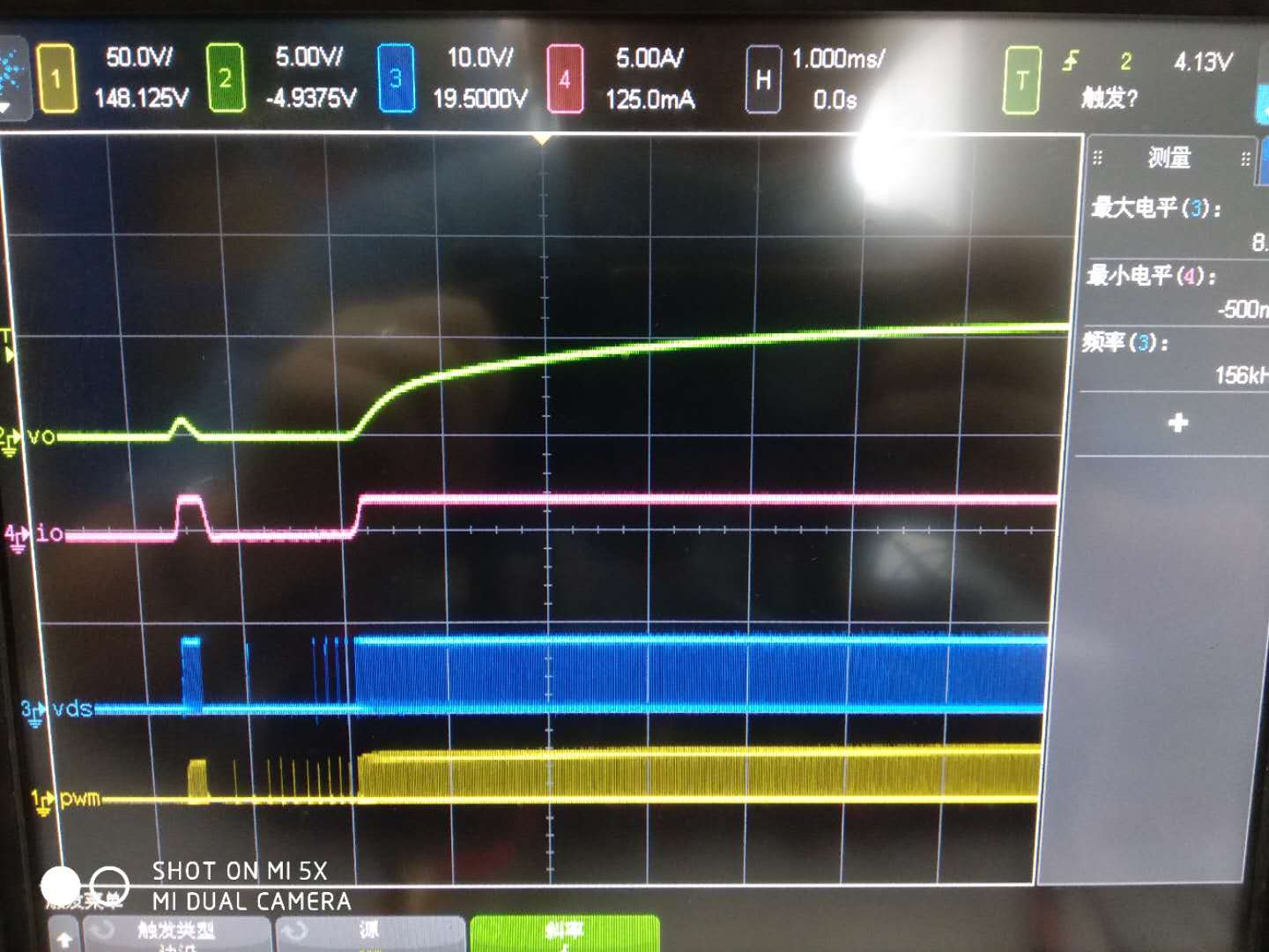
The second abnormal phenomenon is that at the moment of turn-off, the DS pole of the secondary rectifier MOS tube will have a large spike, and the output current Iout will flow in the reverse direction, as shown below:

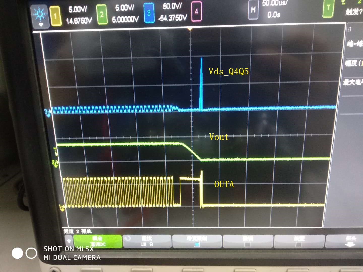
As shown in the figure above, when Vout turns off to 0V, the DS pole of the secondary rectifier will produce a spike of nearly 100V. I do n’t know how to eliminate this spike?

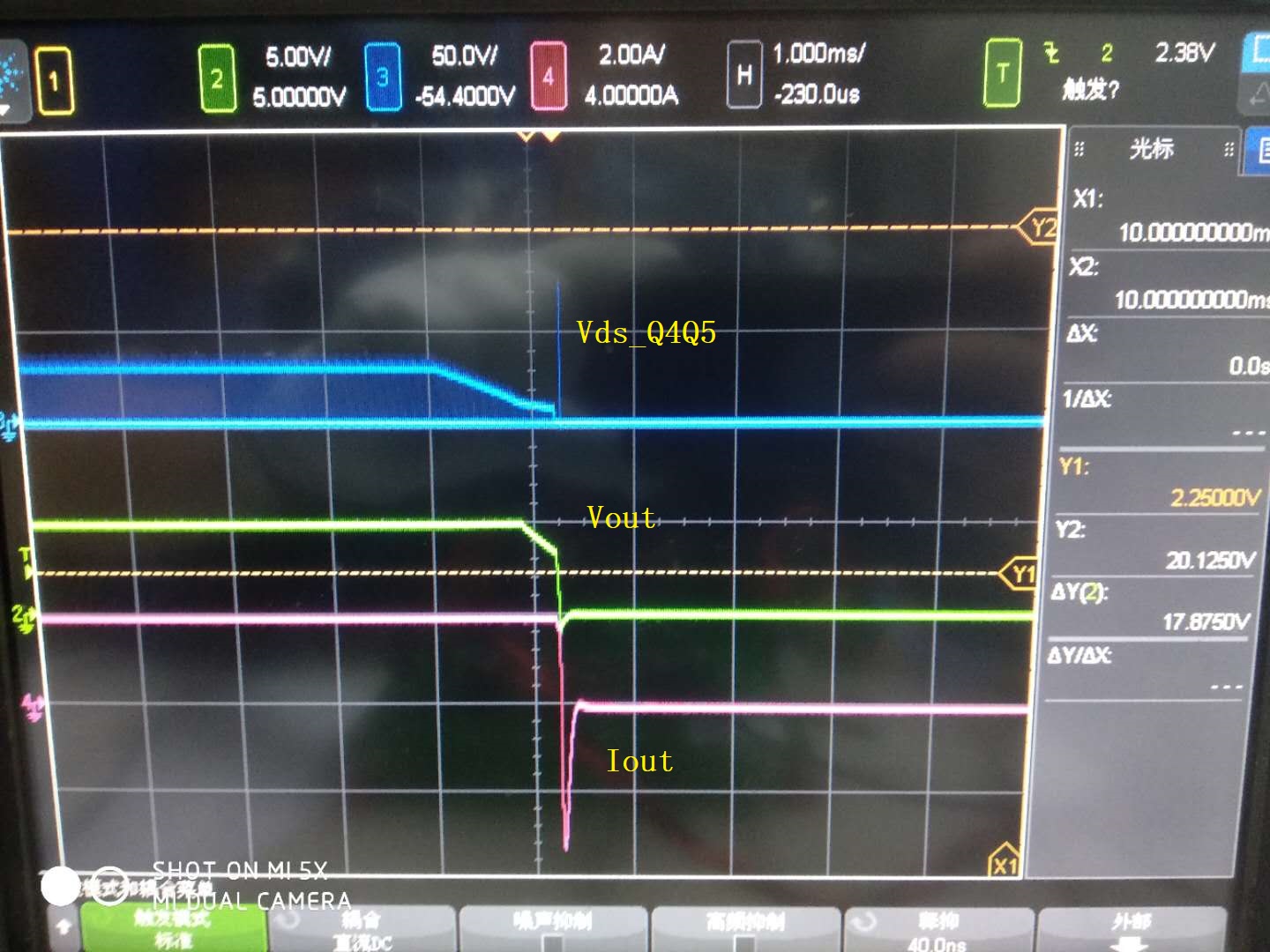
As shown above, at the moment of turn-off, Iout will have a reverse current of 3A, how to eliminate this reverse current?
Please also advise, thank you.

  • Is this reverse current and voltage spike caused by the synchronous rectifier driving when it is turned off, the rectifier is in the on state, and the current flowing through the inductor is reversed?
    How to suppress the current in this direction, especially the spike on the SR, that spike is too large and will break through the SR.
    I have not seen the light-load or no-load shutdown waveforms in the LM5035 manual and application report. I do n’t know what to do to suppress the current reverse flow and voltage spikes?

  • Hi zoujiangyilang,

    Thank you for your post.

    I need to test EVM before answering your question, please allow a little delay.

    Regards,

    Teng 

  • after reducing C20 and C23 to 0.01uF, the spike was eliminated.

    It may be the oscillation caused by the sudden discharge of the energy stored in C20 and C23 when it is turned off.

    I don't know if there is this oscillation on your demo board.

    Why do you want to add C20 and C23, and what is their role?

  • There is another question to ask.

    Startup abnormal phenomenon, as shown below:

    The two figures above are the waveforms at the instant of startup. Before normal startup, the output voltage will have a small tip, and the secondary SR drive will have a cluster of PWM.

    I used to think that this tip was not very big, and there was nothing abnormal on the SR, so I didn't care about it.

    I don't know what caused this abnormal start-up, what caused it?

  • Hi zoujiangyilang,

    Sorry for the long time delay.

    There is already DC block capacitor at primary side, C20 and C23 is not necessary here in my opinion. I am not very sure why designer added C20 and C23 here, maybe it is for quick turn off.  Could you check if INA and INB pin signal of LM5110  are same with SR1 pin signal and SR2 pin signal of LM5035. 

    In our new demo board, it uses digital isolator Si8420BB instead of transformer isolator.

    Regards,
    Teng

  • Hi zoujiangyilang,

    Thank you for you question.

    I also can see this start up waveform on our EVM board, I'd like to have an investigation about this. 

    let's move to the email discussion, my email is teng-feng@ti.com                      

    I am closing this post. 

    Regards,
    Teng