This thread has been locked.

If you have a related question, please click the "Ask a related question" button in the top right corner. The newly created question will be automatically linked to this question.

LM25141-Q1: How to confirm the LM25141-Q1 is working

Expert 1045 points
Part Number: LM25141-Q1
Other Parts Discussed in Thread: LM25141, LM2672

Hi sir,

    Without considering the circuit of backward stage MOSFET ,how do i confirm the LM25141-Q1 is working normally?Or rather,after powering up what kind of signals should be measured then i can confirm the LM25141-Q1  work well。

  • Suy,

    PMP15019 has test results showing proper operation.

    -Sam

  • Hi samuel,

        I measured my LM25141 board(according Vout=3.3v setting) today,please look at the tsst results of below:

        1,The VDDA&VCC are 5V output,but sometimes the VDDA output is only 2.8V,and the SW,HO,LO are no output

         2,When HO&LO output normally the VDDA&VCC are drop about 1V

         3,When Vout is 3.3V the amplitude is not  constant,between 3.3v and 3v

    Could you help me to confirm whether the schematic is correct?

    3632.Power.pdf

  • Suy,

    Your schematic shows VDDA connecting the feedback node of the LM25141 through a 0-ohm resistor (sets 3.3VOUT) but it's also connected to the 5V output of the LM2672 through a 0-ohm resistor. This will hinder the regulation. Is this second 0-ohm a DNP? If not, try removing that resistor.

    -Sam

  • Sam,

       Yes,the resistor is DNP. For the moment the output of HO is not correct,and LO&SW are not output,could you give me some advice on debuging?

        Thanks you

  • Suy,

    I've noticed a few more possible issues on your schematic:

    1. CIN is 470nF on the input of the LM25141-Q1. There's more capacitance on the same node but it may be too far on the layout to benefit the LM25141-Q1. Please try placing 10uF of additional capacitance on the input.

    2. VCCX should be grounded as required in the datasheet.

    Please share waveforms showing HO. I'd like to see what you mean by not correct.

    Thanks,

    -Sam

  • OK, i will send it to you later

  • Hi Jaffe,   

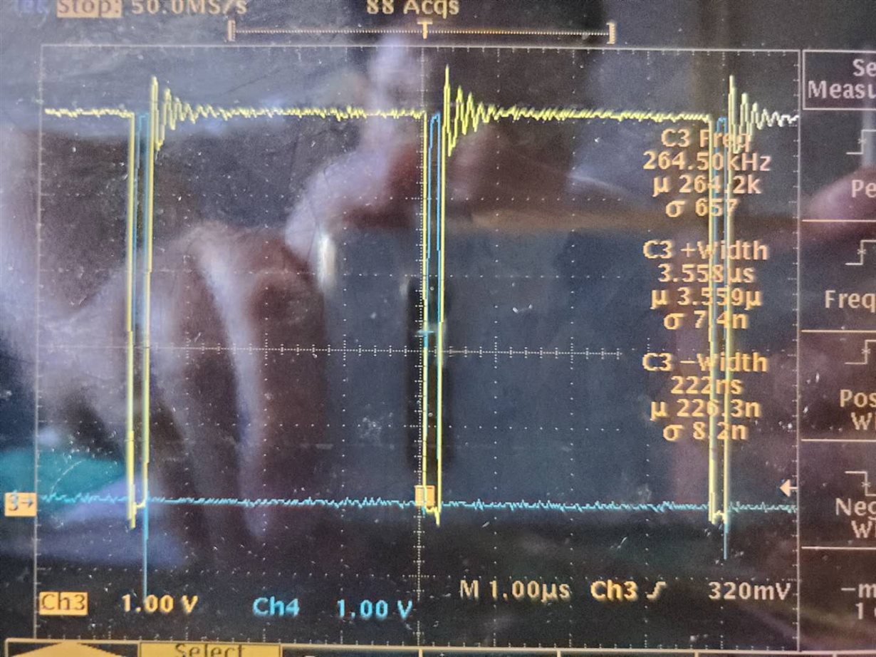
      I measured the HO&LO waveform,pls look at the figure below:HO output(yellow),LO output(blue)

       But i'm very puzzled that the switching frequency is not match to 2.2Mhz which settings in circuit,also the HS & LS MOSFET switching time is not correct according to the duty cycle(Vin=12V,Vout=3.3V).

       Do you think what could be the problem?

  • Suy,

    That's very interesting, I'd expect yellow to be LO and blue to be HO for a 12V to 3.3V duty cycle. Please also share the waveform of SW and VOUT during this condition. So far I'm not sure how this would happen.

    -Sam