This thread has been locked.

If you have a related question, please click the "Ask a related question" button in the top right corner. The newly created question will be automatically linked to this question.

LMG5200: VIN, PGND, SW short

Part Number: LMG5200

Hi all,

I'm trying to evaluate the LMG5200 on an in-house PCB (single layer) and VIN, PGND, and SW short when I apply 28VDC at VIN.  I've verified AGND and PGND are electrically isolated on the PCB and have been using a 677R load to PGND.  The circuit seems to work perfectly up to VIN=25VDC but fails at VIN=28VDC.  Does anyone know what I'm doing wrong here?

LI and HI are 100kHz, 5Vp, 30%DC pulses, offset to create 2uS deadtime.

VCC is 5VDC with 20uF to AGND.

Bootstrap cap is 0.1uF.

VIN has been tested at 12VDC, 22VDC, 25VDC, and 28VDC with 20uF to PGND.

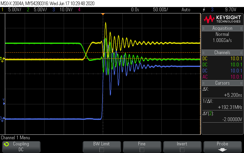
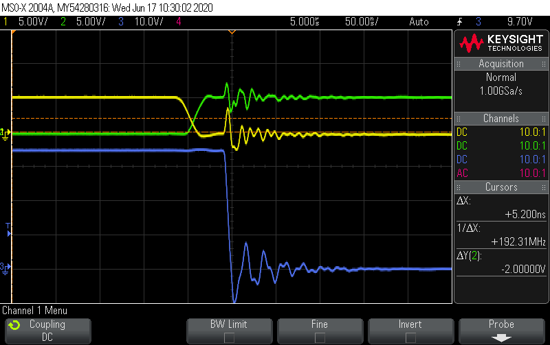
I have noticed not insignificant ringing on the inputs and outputs.  A different forum thread I read suggested this was related to AGND and PGND being connected on the PCB, but this is not the case here.

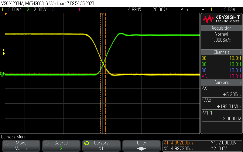
Below is a scope capture of HI and LI v. SW (@25VDC VIN).

  • Hello Nick,

    Thanks for reaching out to us. There are several possibilities that could cause the internal short/damage to the LMG5200:

    1. Overvoltage of the device. Since our device is rated for 80V, and the pulsed voltage could be 100V, the possibility of this happening with 28V input is very low. Nevertheless, it would be good to zoom in the switch node waveform and look at how much voltage overshoot there is. If it is very significant, then it could be a possibility.

    2. Shoot Through. It will happen when the ringing of the HI and LO signal causes unintentional turn on of the both devices. Just to make sure, did you put bypass cap for both input pins? Any high spikes of signal you observed could potentially cause shoot-through of the device? The threshold for high should be around 2V.

    3. Over-temperature. The 2us seems too high. For such a long dead time, the GaN FET will be running in third-quadrant mode and could cause a lot of power loss and heat. Could you shorten the dead time? 

    Also one thing I'm trying to understand is that why the switch node voltage ramp down so slowly during turn-off? Should not the load current discharge the cap pretty rapidly? 

    If you could share the schematics and load current information that would help as well. If you have spare part of LMG5200, it would be good for you to replace the part and test at the lower voltage again. This time, try to monitor the temperature of the FET and see if it behaves normal at lower voltages.

    Thanks!

    Regards,

  • Hi Yichi,

    Thank you for the reply.

    1.) The worst overshoot I saw on the output was 8V on a 25Vdc VIN, which should be well within the 80V spec.  I seem see an average of 3V overshoot on the 5V input.   The attachment on my first post is should illustrate this.

    2.) The last couple tests I ran, I omitted the HI and LI bypass caps but previous tests used 10pF and seemed to fail in the same way.  I'll populate these on the next test.

    3.) I can absolutely shorten the dead time.  It sounds like I underestimated the third quadrant effects here.

    In the screenshot above, the switch node is only connected to PGND through a 677ohm power resistor (no other caps or inductors).  The goal was to determine if these extra components were improperly sized and causing the misbehavior.

    Attached should be a capture of my test schematic.  I have more parts on order and will update once I've run a couple more tests.

    Thank you,

    Nick

  • Hello Nick,

    Looking at the schematic, I don't see too much problem since it follow nicely as our reference design. One improvement can be made is by using more smaller ceremic caps for the power loop instead of two large ones to widen the traces for the power loop and reduce the inductance. However, since the overshoot is very reasonable, I don't think it's a big problem here.

    Also for the resistor you are using, the current level should be fairly small. For now, I think populate the bypass cap for IN pins and repeat the tests with new parts while monitoring the temperature would be the next step.

    Feel free to update us on the results.

    Regards,

  • Hi Yichi,

    I populated another three test circuits, with input bypass caps, and saw similar behavior.  Input pulses were configured for 4.8ns (HI) and 5.2ns (LI) deadtime.

    The first circuit I ran with no output inductance or capacitance, only 677ohms to PGND.  This circuit was able to switch 34Vdc at VIN successfully, but failed when power cycling.  The failure mode presented was VIN, PGND, and SW all shorted with <1ohm.  I neglected to install a thermocouple on this unit, so no temperature data.  When testing this circuit, I started VIN at 10Vdc and increased in 5Vdc steps to 34Vdc.

    The second circuit was run with 4.7uH and 20uF between SW and PGND, in addition to my test load.  This circuit failed when VIN was increased to 20Vdc and its failure mode presents as VIN and SW shorted with <1ohm.  No temperature data for this unit, either.  This circuit I powered on at VIN=20Vdc and seemed to fail as soon as inputs were applied.

    The third circuit was also run with output R, L, and C.  This circuit also failed at 20Vdc, but shows a short from SW to PGND.  This circuit idled (no HI or LI input) at room temperature (23C, in this case) and rose through 30C when inputs were applied, but seemed to fail immediately after inputs were applied.

    Below should be screen captures of my pulse inputs and the first circuit switching at 34Vdc. Pulse deadtime measurements were taken directly from the signal generator.

    I noticed the high side switch features ringing with much larger amplitude than the low side switch. 

    Note, yellow is HI, green is LI, and blue is SW.

    Any help is appreciated at this point.

  • Hello Nick,

    There are two problem I could spot here. First one is the dead time is too short and might have chances to cause shoot-through. You might leave the dead time to be 20-30 ns since there will be delay mismatching in other component. Second one is the power loop inductance. Looking at the switch node waveform, it seems that there will be a large power loop inductance. The HI, LI and SW ringing could be another reason device fails. While using single layer is increasing the inductance, you might still want to take a look at the layout and minimize the length and widen the power loop trace.

    Hope this helps.

    Regards,