This thread has been locked.

If you have a related question, please click the "Ask a related question" button in the top right corner. The newly created question will be automatically linked to this question.

LM5143-Q1: Power management forum

Part Number: LM5143-Q1
Other Parts Discussed in Thread: LM5143
Dear,
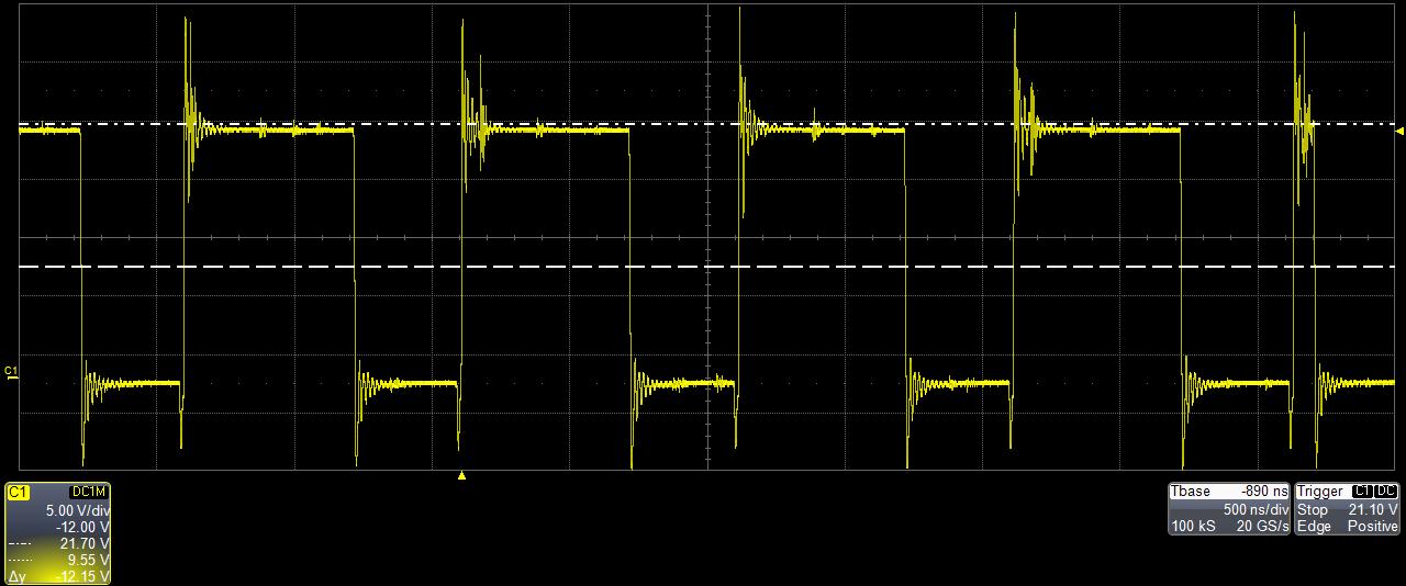
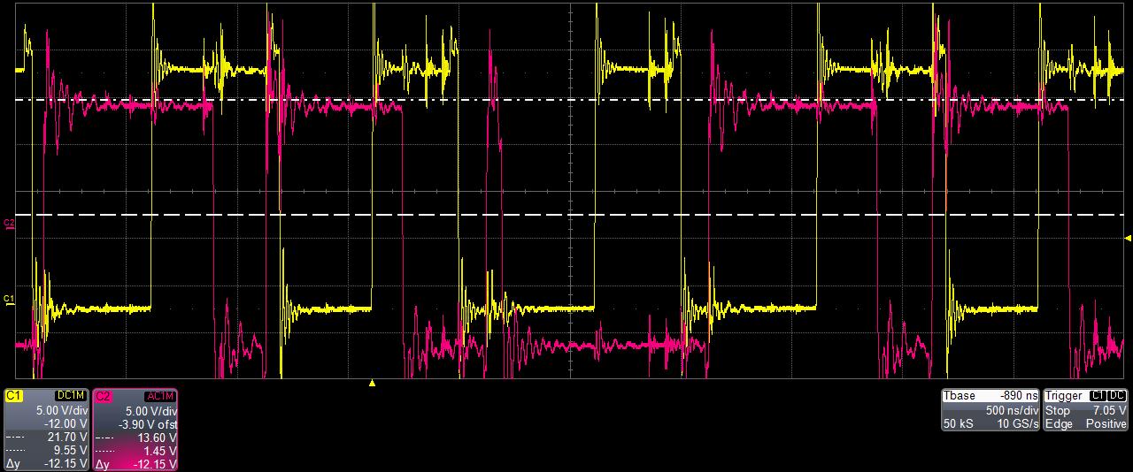
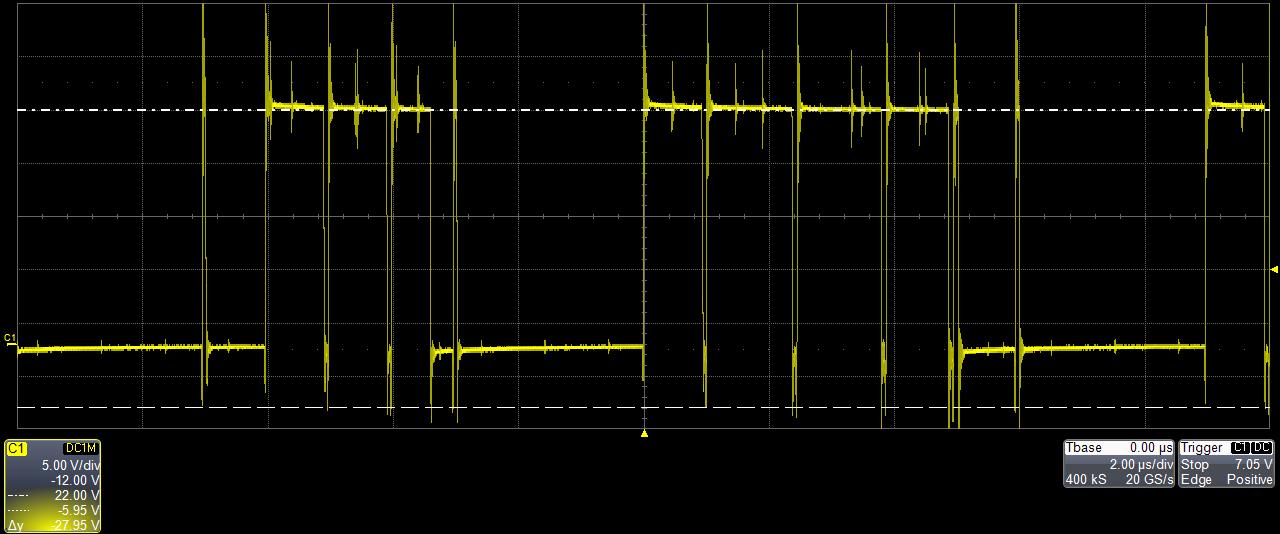
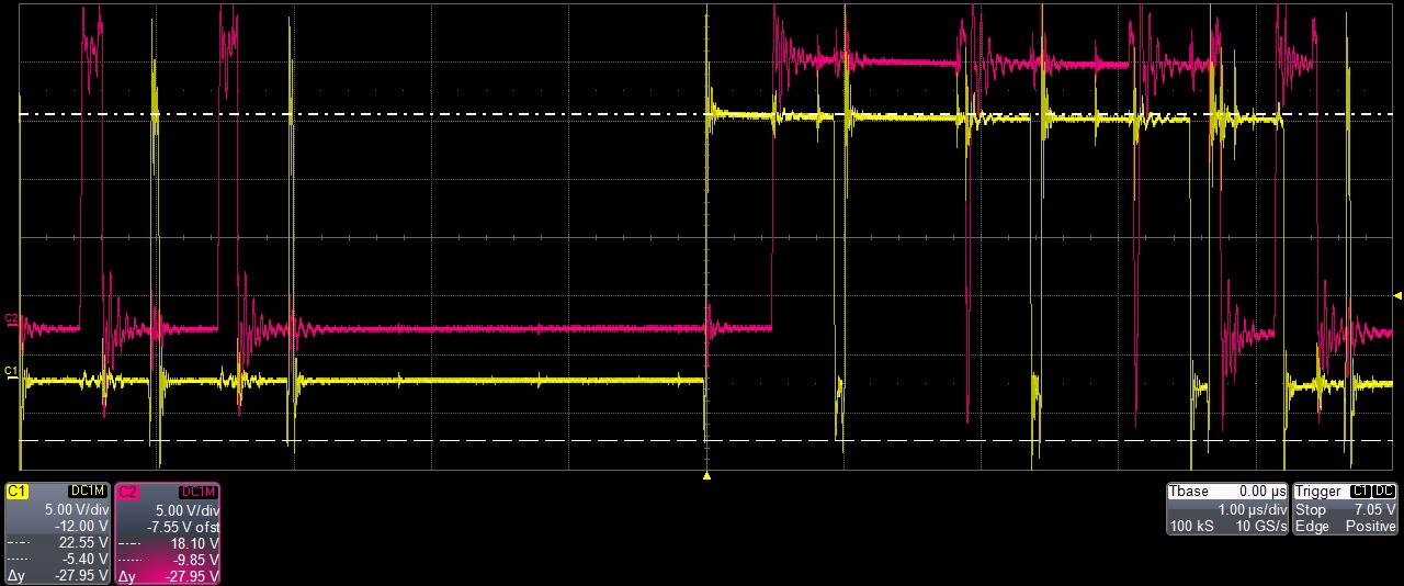
The problem is that after power on or pulling EN high, the controller remains stuck in the start-up mode (still in DCM/DEMB mode, but not necessarily in hiccup mode) with output voltage just below the set/regulated output voltage. Placing a 100 pF capacitor over the current sense input does help, but start-up is still far from reliable. In a case the controller enters the normal operating mode, everything works as expected with proper voltage regulation and sufficient output current, etc.. I also experimented with  increasing Ccs capacitor from 100n to 1uF (and Rcs from 36K to 3K6) with no success.
What else can I do to improve the situation?
In the design, relative large inductors are used (10..15 uH). Because of the large inductor components, the current sense tracks are relatively long but they are routed in parallel. 
On board several LM5143 controllers are placed for 12V/40A (2-phase), 3V3/10A and 5V/10A power., all with more or less the same start-up problem. The Rcs and Ccs values have been calculated using the guidelines in the datasheet. GanFETs (EPC2102) are used instead of MOSFETs.
  • Hi

    below is some comments:

    1. GanFETs have very fast dv/dt when it turn on/off, which may interfere the current sense and the control block of the chip( you may need very pay attention to the layout)

    2. Current sense need to place as differential way, the ground should embrace the current sense trace to make it not interfere by the noise souce

    3. LM5143 is designed for drive mosfet, it don't have internal clamping circuit in the driver for protecting the GS of GanFET.

    4. Can you uploading the issue waveform including SW, IL as well as schematic?

    Thanks

  • Hello Daniel,

    Thank you for your quick response.

    Next to placing a 100pF capacitor accross the current sense input, removing the soft start capacitor also improves start up behavior.

    1. I measured a dv/dt of approximately 25V/ns (with 20..30V input voltage). What is the limit for the LM5143? It is probably a good idea to insert a gate resistor for the high side FET to limit the dV/dt. EPC recommends at least 1 to 3 ohms.

    2. The current sense traces are routed on the top signal layer, not completely surrounded by ground traces. We can probably route the current sense traces on an internal layer.

    3. Yes, you are correct. For the final design I am planning to place free-wheel diodes and 4.7V zeners on the high side gates.

    4. Attached is part of the schematics (the 2-phase 12V/40A power supply unit). Waveforms are attached also. Please note that I used a standard probe grounding clip 

    - Trace 1 is the SW1 voltage of driver U400 driver 1 in case the output voltage is OK. Note the sudden change in duty cycle.

    - Trace 2 are the SW1(y) and SW2(r) traces in case the output voltage is OK.

    - Trace 3 is the rising edge of SW1, output voltage is OK

    - Trace 4 is the SW1 voltage in case the output voltage is NOK (approximately 10V instead of 12V)

    - Trace 5 are the SW1(y) and SW2(r) voltage traces in case the output voltage is NOK.

    - Trace 6 is the output voltage at the L400-L401 node

  • Hi

    pls my suggestion

    1. it looks only Vo have electrical cap , which will easy to get noise and go into the current sense PIN(VOUT1, VOUT2), suggest put more ceramic cap which is low impedeance at high frequency can help filter the noise at output
    2. short L402, the two stage of L C filter will not good for the loop stability
    3, I can't see the compensation value very clearly, use caculator to see whether the loop compensation is good, and you can also increase the Ccomp and decrease the Rcomp to reduce the bandwitdh to see any help
    4. put more ceramic cap at input , and make sure there is bypass capacitor nearby the Vin pin.