This thread has been locked.

If you have a related question, please click the "Ask a related question" button in the top right corner. The newly created question will be automatically linked to this question.

LM5122-Q1: Ti Boost Converter Selection

Part Number: LM5122-Q1
Other Parts Discussed in Thread: LM5121-Q1, LM5122, LM5121, LMG5200, LM5114, LMG5200EVM-02, LMG1210, LM51561, LMC555, PMP11112

Hi,

I'm trying to select an appropriate Boost Converter for a new product design. The design input uses (6) 18650 Li-Ion cells in series with the pack specification below:

Battery Spec:

Output pack voltage = (21 - 25.2)vDC
Nominal pack voltage = 22.2vDC
Continuous pack current= 30A

----------------------------------------------

I'm looking for the following output:

Boost Spec:

Output voltage = 65vDC
Output current = 7.5 to 8 Amps

I need this design to be a small as possible and have large heat-sinking options. With that in mind, I've identified (2) Controllers that may work the LM5122-Q1 OR LM5121-Q1. So my questions are:

1) Are the (2) Controllers I've identified the best for this application

2) I've started a Webench design with the LM5122-Q1, but it doesn't look as though you can run a multi-phase design using this tool. I think this application might require such a design.

Please let me know your initial thoughts.

-Thank You,

  • Hi Kyle,

    Thanks for reaching out with your questions and for considering the LM5122  and LM5121.

    Based off of the specifications provided I think these are the correct parts for the application. The power levels is pretty high (520W) I suggest using a two phase design. With a two phase design the switching frequency can be increased and this will help reduce size of the inductor and output capacitors. A two phase design will also help with the thermal management as the power dissipation is spread out.

    To run WEBENCH I suggest just running the power requirements at 1/2 as it is a two phase design. This will help find the correct power train components. PMP7979 is a good reference on how to connect the LM5122 in a multi phase design.

    Please let me know if you have any questions.

    Thanks,

    Garrett

  • Hi Garrett,

    Thanks for getting back to me. Glad I'm on the right track with the LM5122 in a multi-phase configuration.

    Is this Controller capable of driving GaN FETs?
    If so, should I consider using them here in this design to achieve a higher switching frequency with this controller? Webench doesn't offer this functionality.

    I've found a low-profile inductor from KEMET that seems to meet more than the requirements that Webench has put out so far and its Spec Sheet talks about using it alongside GaN FETs to potentially drive it at higher frequency. This might substantially lower the number of capacitors that I need as Webench won't go any higher of a frequency than 337kHz.

    I've noticed that Ti sells the LMG5200 and it is an integrated Half-Bridge that uses GaN FETs. Is this component compatible with the LM5122 as the driver?

    Thanks Garrett!

  • Hi Garrett,

    Still trying to figure out if the LM5122 is the correct Boost Controller for this project. More specific questions:

    1) Does the LMG5200 make sense to use with the LM5122?

    2) Does the LM5122 support 6v output from the H/L drivers to drive discrete GaN FETs?

    3) If the LM5122 supports driving 6v from the H/L drivers, how is that implemented?
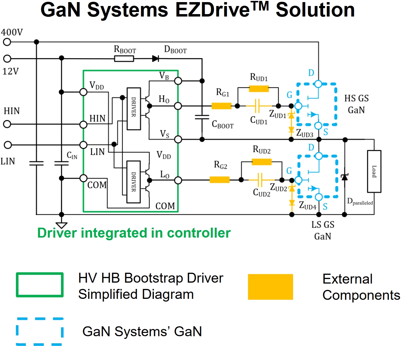
        I've pasted the gate drive example from GaN Systems, but this may not be necessary if the gate drive voltage can be lowered to support 6v operation.

    4) If the EZDrive implementation is required, how will that look in the schematic here? I ask because the example above assumes a gate drive voltage generated off the Controller and this is not the case with the LM5122.

    5) Do you think I can push the LM5122 to operate close to 1MHz using GaN? I was looking in the data sheet and it says with Rt tied to 10kOhms, the MAX frequency generated is 875kHz.

    Thank You,

  • Hi Garrett,

    So I believe I've found part of one of the answers in the datasheet.

    #3) It looks like the LO driver is derived from VCC and is driven at 7.6v to the LO pin:

    "7.3.2 High Voltage VCC Regulator

    The LM5122 contains an internal high voltage regulator that provides typical 7.6 V VCC bias supply for the controller and N-channel MOSFET drivers. The input of VCC regulator, VIN, can be connected to an input voltage source as high as 65 V. The VCC regulator turns on when the UVLO pin voltage is greater than 0.4 V. When the input voltage is below the VCC setpoint level, the VCC output tracks VIN with a small dropout voltage. The output of the VCC regulator is current limited at 50 mA minimum."

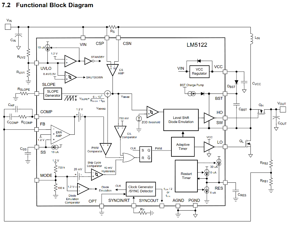
    Also from the

    it seems that the HO pin will provide 7.6v or the BST Charge pump voltage if it is higher.

    If that is correct, is it possible to get the H/L side to drive at 6v for safe GaN operation?

    I could really use some help figuring this out.

    Thank You,

  • Hi Garrett,

    Any update on this?

    Thanks,

  • Kyle

    The LM5122 will not drive GaN FETs as it is design for standard silicon MOSFETs. This is very important as the GaN FETs have a very low threshold voltage and driving them with a standard driver could result in shoot through issues. That being said something like the LMG5200 can be used if your application needs GaN FETs. The LM5122 has a maximum operating frequency of 1MHz.

    Please let me know if you have any questions.

    Thanks,

    Garrett

  • Hi Kyle,

    Sorry for the delay. 

    I would not recommend controlling the output of the VCC regulator. This is because you may be able to control the input to the VCC regulator using an external clamp, but you you cannot control the spikes that will occur during the sourcing and sinking of the GaN FET's capacitances. Instead, what I would recommend is to use the LM5122 gate signal as an input into the LM5114, a LO-side GaN FET gate driver, and power it through a LDO or something from VCC. You can also do something similar with the HO FET, but this may require more specialized design. 

    That aside, why the interest in GaN? For the LM5122, the maximum switching frequency is 1MHz, and at 520W power, you can utilize a dual-phase configuration and generate a suitable design even with MOSFETs. 

    Thanks,

    Richard

  • Hi Richard,

    Thanks for sharing that with me. I figured that the LO GaN might be easier to drive, but wasn't sure. Maybe I will stick to MOSFETs for now, but the reason why I'm interested in GaN is for the reduced space that I might be able to get out of it. I'm trying to fit the Boost Converter in a (53 X 46 X 13)mm volume and it has proved difficult so far.

    If you had any more suggestions or comments I'm thankful for the help.

    -Kyle

  • Hi Garrett,

    I'm still trying to figure out a way to successfully use the LM5122 for this application as it still looks like the closest off-the-shelf fit for the application.

    I'm using WEBENCH to design for half the power as you suggested and then will add an additional identical phase for the other half of the power per PMP7979. In WEBENCH, I have the output at 65v and 4A with a "User Sync Frequency" of 646kHz. I'd like to push this switching frequency higher.

    Some followup questions:

    1) I've noticed as the output voltage increases in WEBENCH, the available switching frequency decreases. Why is this?

    2) Additionally to get the highest available frequency at these higher output voltages, I have to use a "User Sync Frequency" which enlarges the circuit. It no longer seems that WEBENCH thinks the LM5122 can generate these higher frequencies itself. Is there a way to avoid this issue other than lowering the output voltage?

    3) Would this higher voltage output design (65v out) benefit from some sort of driving isolation and/or external VCC supply to allow the LM5122 to work at a higher self generated frequency closer to 1 MHz?

    Thank You,

  • Hi Garrett,

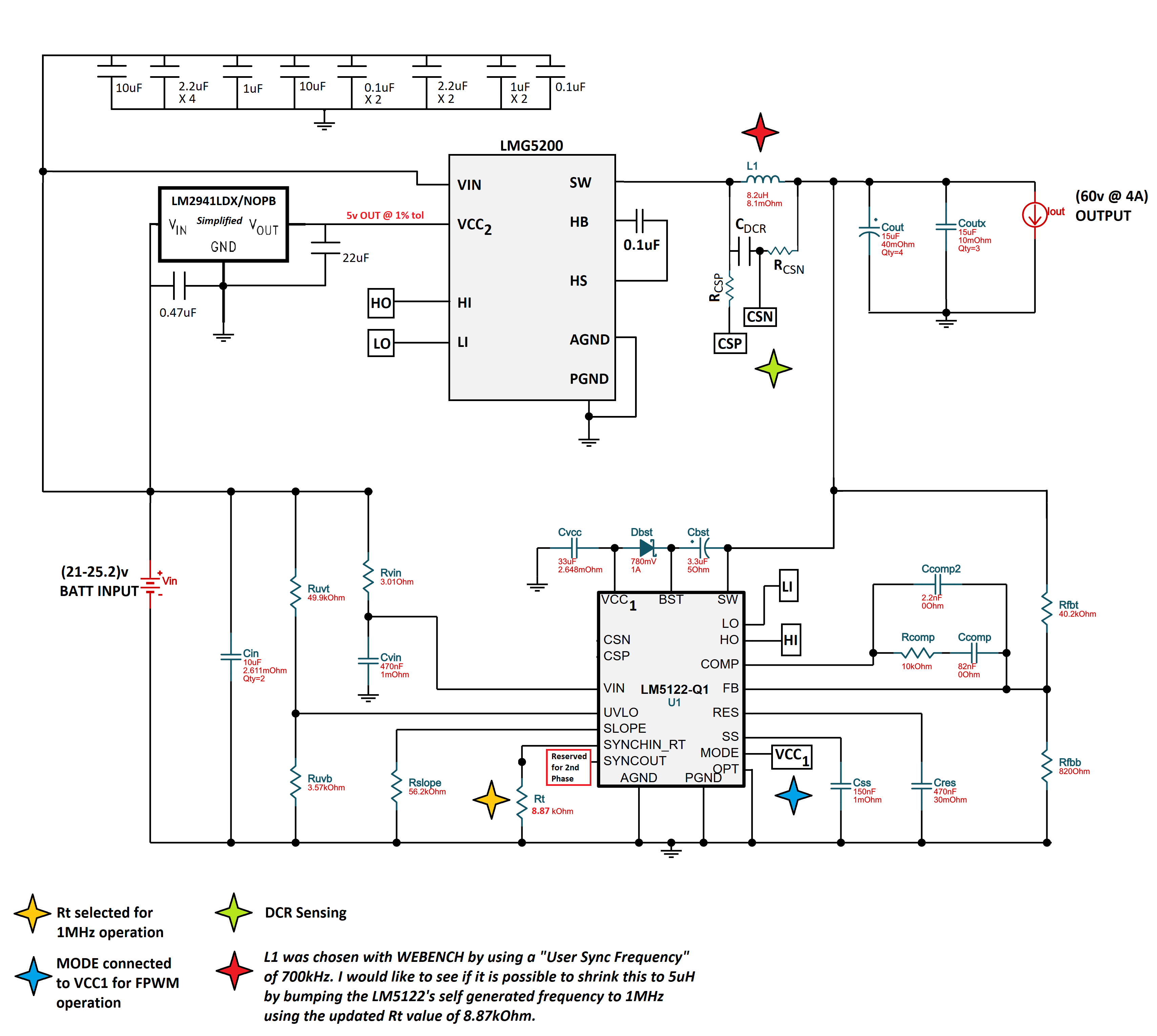
    I've done some more work on getting a functional design together with the LM5122. I am interested in using the LMG5200 to achieve stable higher switching speeds at 1MHz while also minimizing the necessary size of the inductor to around 5uH. I'm trying to do this without raising the heat load substantially but should be able to conduct quite a bit of heat from the surrounding aluminum shell of the device if necessary.

    I still have the other questions form the last post, but I think that WEBENCH was lowering the available frequency that could be generated by the LM5122 at 65v out because of its internal VCC / sourcing & sinking enough current in the LO/HO pins. With that in mind, perhaps the setup below using the LMG5200 will end up being a more robust design at 1Mhz.

    The values tied to the LM5122 had all been picked using 60v out @ 4A and introducing a "User Generated Frequency" of 700kHz. So the 8.2uH inductor was also picked by WEBENCH, but WEBENCH could not pick any MOSFETs that would work for the design for the HIGH/LOW sides and instead had them listed as IdealFETs. Since I was running up against the IdealFETs as well, I thought that the LMG5200 might be a good path to pursue.


    Questions:

    1. Generally speaking, is everything connected correctly to begin thinking about prototyping?
      For instance, is the SW node coming from the LM5122 in the right position?

    2. I used the LMG5200EVM-02 GaN Half-Bridge PowerStage EVM as a reference to connect the devices. There was a "Dead-Time Generating Circuit" in the EVM schematic, but I left it out for now since I thought that the LM5122 adjusted the Dead-Time on its own. Is that correct?

    3. Is the boot-strap circuit connected to the LM5122 necessary any longer since it will be driving the LMG5200 which has its own internal boot-strap circuit for the HIGH GaNFET? If it is not needed how should VCC1, BST & SW on the LM5122 be connected?

    4. I've connected the MODE pin to VCC1 of the LM5122 to run the device in Forced-PWM since I was interested in fast light to high load operation as well as DCR sensing. Do you see any major downside to doing this?

    Thank you for your help!

  • Hi Garrett,

    Any update on this?

    Thank You!!

  • See Comments Below

  • Hi Kyle,

    For future correspondence, I will be responding to your inquiries on this thread.

    To answer your first comment regarding the WEBENCH:

    1) I've noticed as the output voltage increases in WEBENCH, the available switching frequency decreases. Why is this?

    This could be due to the LM5122 minimum LO off-time. As your output increases in a boost, your duty cycle also will increase- so to maintain within the datasheet limitations, the frequency will be lower. 

    2) Additionally to get the highest available frequency at these higher output voltages, I have to use a "User Sync Frequency" which enlarges the circuit. It no longer seems that WEBENCH thinks the LM5122 can generate these higher frequencies itself. Is there a way to avoid this issue other than lowering the output voltage?

    The addition to the schematic is a SYNC input in series with a Csync capacitor, which is in parallel to the Rt pin. From working with Webench, I am not able to avoid this same issue. Please see section 7.3.11 in the datasheet for more clarification. 

    3) Would this higher voltage output design (65v out) benefit from some sort of driving isolation and/or external VCC supply to allow the LM5122 to work at a higher self generated frequency closer to 1 MHz?

    There usually is no need to implement a driving isolation/external VCC at 65V in order to operate at a higher self generated frequency. Adding external VCC reduces internal power dissipation, and driving isolation can be done with the LM5122 in a flyback configuration. 

    Thanks,

    Richard

  • Hi Richard,

    Thank you for getting me the information about the self generated frequency capability, which isn't really talked about in the datasheet. Also, these forums are a bit confusing to use, for instance, at the bottom of your last message one of your comments came through to my email but isn't shown in this forum,

    "To answer your second comment regarding the LMG5200:

    First and foremost, your size requirements for this board is already very small for this design. Secondly, LMG5200 is primarily used in a buck and buck-derived topologies, and you may run into some issues with making sure the dead-time is suitable for both the LM5122 and LMG5200. In this case, I would not recommend using the LMG5200 here since it

    1. provides many more design variables and
    2. may not necessarily be the best part for the job here."

    Questions:

    1. So just to recap, the LMG5200 should not be used for BOOST Designs only Buck Designs. With that in mind, do you think a part like the LMG1210 driving discrete GanFETs like the EPC2022 would be more suitable?

    2. For instance, the LMG1210 allows the control of dead-time directly but this still doesn't really seem to solve the issue with the LM5122 being unable to drive with a self-generated higher frequencies approaching 1MHz.

    3. Would you recommend using the LM51561 instead and forgetting about splitting the power among (2) phases as planned with the LM5122?

    Thank You Richard!

  • Hi Kyle, 

    Sorry for the confusion. I did some digging into the part again, and decided to edit my comment in order to make sure the recommendation is as clear as possible. 

    First and foremost, let's go back to the LMG5200 to clear up your questions:

    1) Generally speaking, is everything connected correctly to begin thinking about prototyping? For instance, is the SW node coming from the LM5122 in the right position?

    Unfortunately, the connection is not correct. First and foremost, in order to implement the boost, you would need to make sure that VIN pin of LMG5200 should be connected to the output of the boost converter, and the SW pin should be connected to the inductor and input voltage of the converter. Additionally, since the LMG5200 inputs take TTL level, the SW pin of the LM5122 will need to be grounded in order to not damage the inputs of the LMG5200. Because of this, I'm unsure of the behavior of the adaptive dead-time circuit. What you can do is follow the LMG5200 and LMG5200EVM-02 guideline to carefully control the input to prevent shoot-through conditions.  

    2) I used the LMG5200EVM-02 GaN Half-Bridge PowerStage EVM as a reference to connect the devices. There was a "Dead-Time Generating Circuit" in the EVM schematic, but I left it out for now since I thought that the LM5122 adjusted the Dead-Time on its own. Is that correct?

    Since SW pin of LM5122 is grounded, the LM5122 cannot adjust the dead-time on its own. 

    3) Is the boot-strap circuit connected to the LM5122 necessary any longer since it will be driving the LMG5200 which has its own internal boot-strap circuit for the HIGH GaNFET? If it is not needed how should VCC1, BST & SW on the LM5122 be connected?

    Boot-strap circuit is still needed in order to generate the HO voltage. VCC should still be connected in order to generate the gate drive signals, SW should be grounded. 

    4) I've connected the MODE pin to VCC1 of the LM5122 to run the device in Forced-PWM since I was interested in fast light to high load operation as well as DCR sensing. Do you see any major downside to doing this?

    FPWM operation is ok. DCR sensing is also okay, though accuracy may be reduced. 

    Secondly, I will answer your question in the previous post:

    1) So just to recap, the LMG5200 should not be used for BOOST Designs only Buck Designs. With that in mind, do you think a part like the LMG1210 driving discrete GanFETs like the EPC2022 would be more suitable?

    This was my misunderstanding with the LMG5200. Both should be doable, as long as you follow the datasheet and application recommendations since the LM5122 has been used in circuits with external gate driver ICs.

    2) For instance, the LMG1210 allows the control of dead-time directly but this still doesn't really seem to solve the issue with the LM5122 being unable to drive with a self-generated higher frequencies approaching 1MHz.

    Unfortunately, this is a limitation with the LM5122's maximum frequency. 

    3) Would you recommend using the LM51561 instead and forgetting about splitting the power among (2) phases as planned with the LM5122?

    It might be easier to just do this with the LM5122 at 1MHz switching frequency if you want to use the LMG5200. You will just need to make sure that you do not violate the minimum off-time, which is calculated as (1-D_max)*1/(fsw), and D_max is calculated as 1-Vin_min/Vout. 

    Thanks,

    Richard

  • Hi Richard,

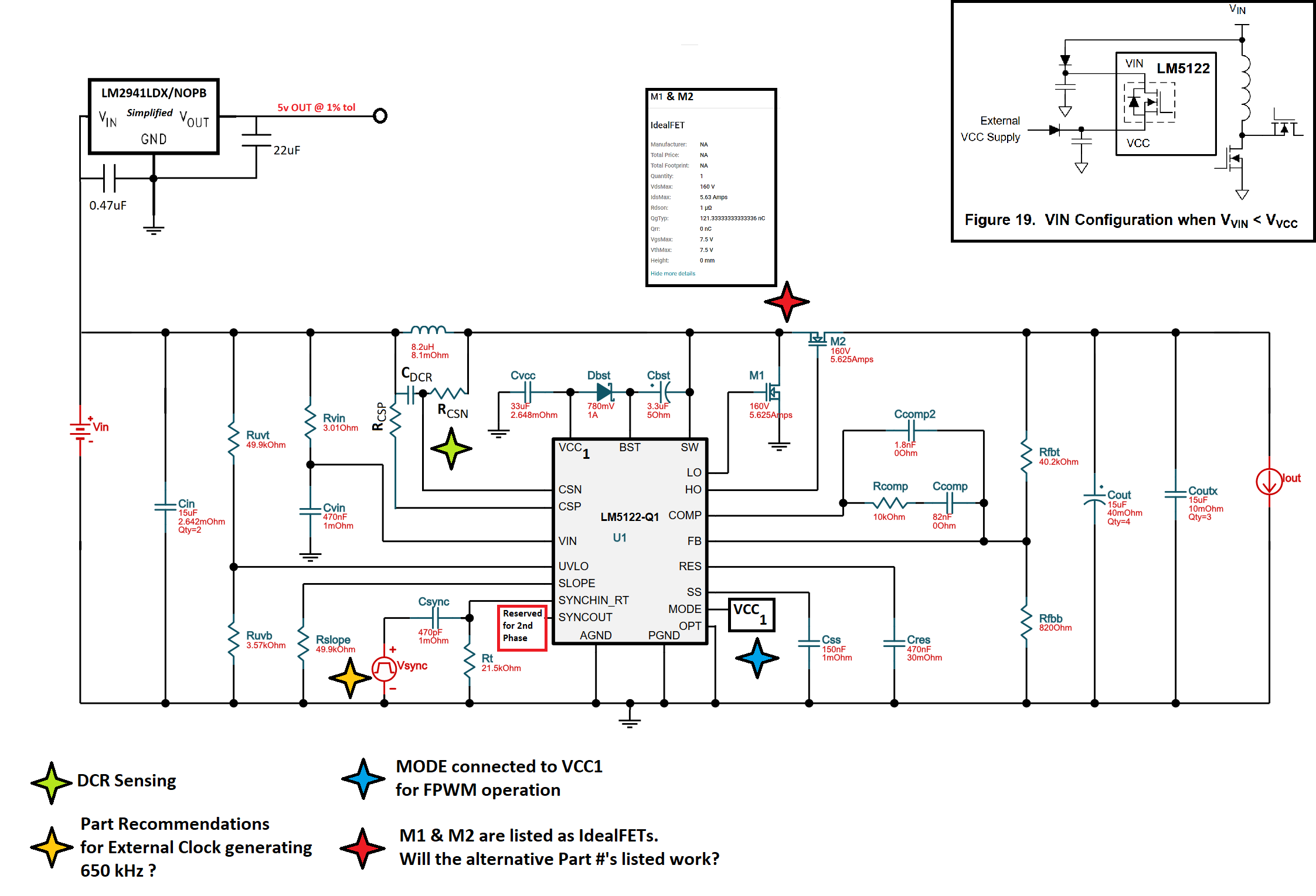
    Thank you for answering my previous questions. I've modified my last design to include some of the previous concerns expressed especially where GaN seems to be hard to implement in this design.  I think getting a working design with Si MOSFETs and an external clock will be the easiest path for now. I can improve the design as I go. Below is the updated circuit diagram with the following specs: (21 - 25v) input, 60v @ 3.75A output, & external clock of 650 kHz.

    My questions mainly focus on implementing the correct N-Channel MOSFETs and the correct external clock.

    Questions:

    1. Is the BSC500N20NS3 G a good choice for the HI/LO N-Channel MOSFET for this design?
      It has the following specs:
      1. Vds: 200v
      2. Id: 24A
      3. Vgs: +/- 20v
      4. Rds On: 0.042 ohm
      5. Vgs th: 2v
      6. Qg: (15nC typical) - 20nC
      7. Pd: 96W

    2. If this is an appropriate choice for the MOSFETs, can it be added to WEBENCH so that it can be selected in my design?
      I'm calculating the I2 losses for the MOSFET to be around ~672mW for 4 Amps per MOSFET.

    3. What optimization parameters should I look for between the HI / LO MOSFET? Should I be looking for a different HI MOSFET than the BSC500N20NS3 G?

    4. I've copied the IdealFET output from my WEBENCH design above the RED star. It says the VgsMAX should be 7.5v, does the chosen MOSFET meet this requirement with a fully ON state of 10v between gate & source or is this referring to 7.5v being the fully on-state?

    5. I'm planning on eventually driving the LM5122 with an external 5v VCC source (LM2941LDX/NOPB) to reduce the LM5122's internal losses. It looks like I need to replace Rvin in the design with an appropriate Schottky diode that can handle the input voltage as well as a Schottky diode protecting the 5v source from the LM2941LDX. Do you see any real gain from doing this? One of the reasons I'm considering it is that I will most likely require an external source to drive the external clock as well so it may make sense to exploit its presence in the design further.

    6. Lastly, I'm driving the LM5122 at a frequency of 650 kHz with an external clock in the WEBENCH design since the LM5122 can't do it by itself. Can you recommend an external clock (P/Ns) for this design and any references?

  • Please see the newest post with updated diagram.

  • Hi Kyle,

    Thanks for providing the updated schematic. Here are my answers to your questions:

    1) Is the BSC500N20NS3 G a good choice for the HI/LO N-Channel MOSFET for this design?
    It has the following specs:

    Vds: 200v

    Id: 24A

    Vgs: +/- 20v

    Rds On: 0.042 ohm

    Vgs th: 2v

    Qg: (15nC typical) - 20nC

    Pd: 96W


    This FET is fine for this application.

    2) If this is an appropriate choice for the MOSFETs, can it be added to WEBENCH so that it can be selected in my design?
    I'm calculating the I2 losses for the MOSFET to be around ~672mW for 4 Amps per MOSFET.

    I'm not too sure how to add this to Webench. Usually to calculate losses, you would want to take the sum of the FET's conductive and switching loss. This article should give an approximate calculation.

    3) What optimization parameters should I look for between the HI / LO MOSFET? Should I be looking for a different HI MOSFET than the BSC500N20NS3 G?

    Usually you would want to focus on rds_on for conduction losses, and Qg for switching losses (please see above article). Usually, larger MOSFETs will have lower rds_on but higher Qg, which means switching losses may take a large amount of losses at higher frequencies. 

    4) I've copied the IdealFET output from my WEBENCH design above the RED star. It says the VgsMAX should be 7.5v, does the chosen MOSFET meet this requirement with a fully ON state of 10v between gate & source or is this referring to 7.5v being the fully on-state?

    LM5122's VCC voltage is 7.6V unloaded, so it will be lower under load. I think that is the reason for the VgsMAX = 7.5V. Your MOSFET has a Vgs_max larger than 7.5V, which is fine. 

    5) I'm planning on eventually driving the LM5122 with an external 5v VCC source (LM2941LDX/NOPB) to reduce the LM5122's internal losses. It looks like I need to replace Rvin in the design with an appropriate Schottky diode that can handle the input voltage as well as a Schottky diode protecting the 5v source from the LM2941LDX. Do you see any real gain from doing this? One of the reasons I'm considering it is that I will most likely require an external source to drive the external clock as well so it may make sense to exploit its presence in the design further.

    You are correct- supplying external voltage to VCC will reduce LM5122 internal losses. However, you should not power VCC externally with a 5V source. External voltage applied to VCC directly should be in between 9V to 14.5V. I think figure 17, 18 and 19 in the datasheet will provide good starting points. 

    6) Lastly, I'm driving the LM5122 at a frequency of 650 kHz with an external clock in the WEBENCH design since the LM5122 can't do it by itself. Can you recommend an external clock (P/Ns) for this design and any references?

    LM5122 can drive up to 1MHz switching frequency. This reference design uses the LMC555 to generate the external clock. 


    Thanks,

    Richard

  • Hi Richard,

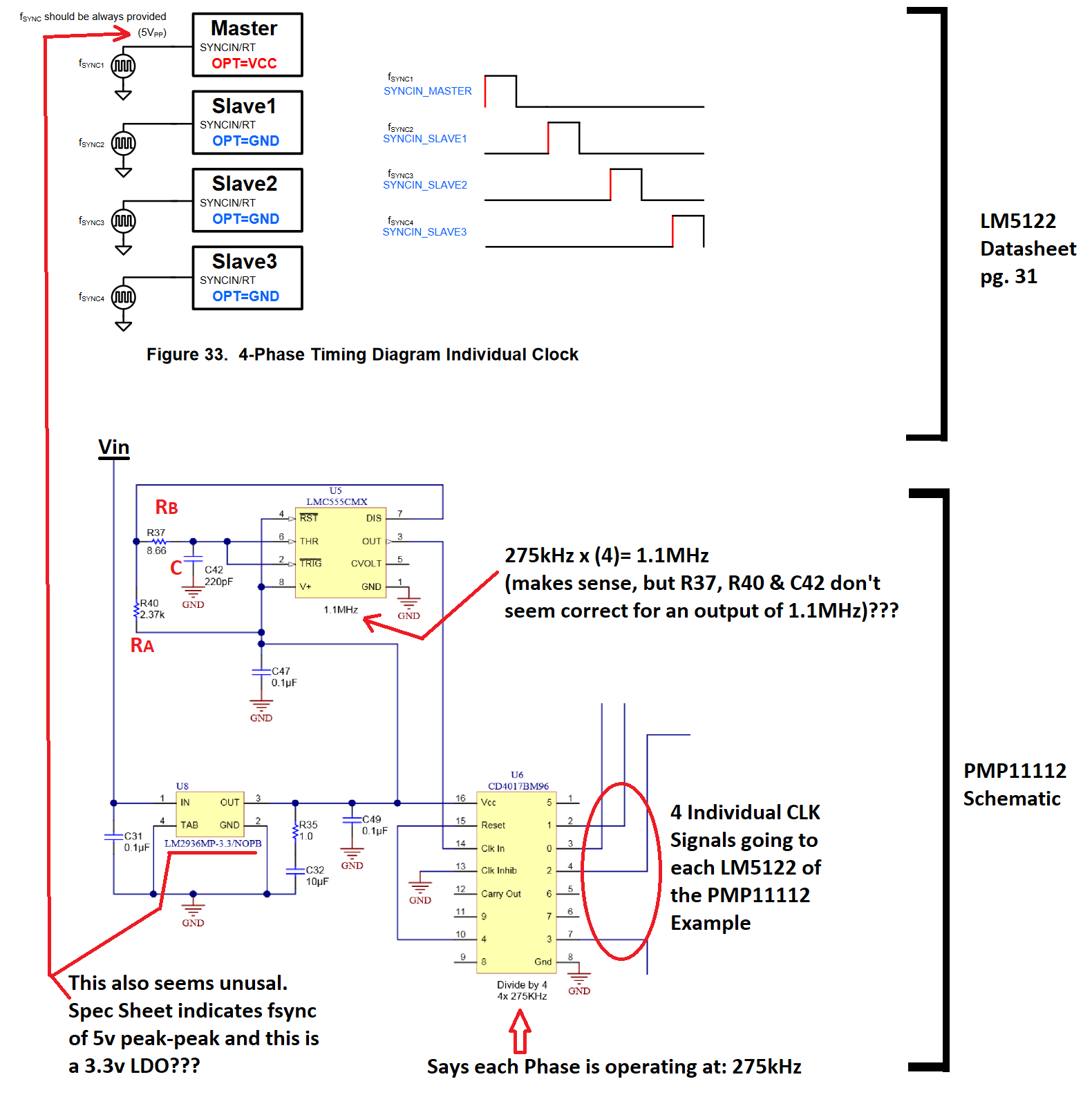
    Thank you for answering my questions, that article you provided was very useful. I have an initial design that I think will work now and give me a good place to start prototyping. I have a few additional questions regarding the PMP11112 reference that was provided to show CLK generation for each of the phases. The image below shows the two areas that are confusing:

    Questions:

    1. The decade counter CD4017 says its dividing the incoming CLK signal from the LMC555 by 4 for an individual phase frequency of 275kHz. That makes sense. When you multiply 275kHz by 4 you get a CLK frequency of 1.1MHz as indicated below the LMC555. Great. However, the confusion begins with the selection R37, R40 & C42...

      I'm pretty sure that the LMC555 is setup in this configuration for Astable Operation.... So the frequency should be given by f = (1 / T) = (1.44) / [(Ra + 2Rb)C]

      When I use this formula, I get f = ~2,741,758.35  which does not seem correct. Am I missing something?


    2. Additionally, it seems that in the PMP11112's schematic there is a Fixed 3.3v LDO providing power to the LMC555 & CD4017. The Spec Sheet for the LM5122 says that a 5v Peak-to-Peak CLK signal should be provided. Maybe I'm misunderstanding this configuration, but wouldn't this be providing a 3.3v CLK Signal to the LM5122s in the configuration?


    3. The duty cycle seems off as well, and from the LMC555's Spec Sheet, D = (Rb) / (Ra + 2Rb)

      I'm getting a Duty cycle of 0.3627% 

      However, if I am calculating Duty Cycle as D = (Ra + Rb) / (Ra + 2Rb)
      I get 99.6372 %


    4. As an exercise, If I am aiming for an individual phase frequency of ~345 kHz with 4 phases, then I should have a CLK freq = 1.380MHz, right?

      Then my Ra = 4.75k Ohms
                     Rb = 8.25 Ohms
                     C = 220 pF
                    
                     CLK freq = 1.376 MHz  -> divide by 4 = 344kHz individual phase frequency

      Or am I missing something from the schematic?

  • Please see the newest post with updated diagram

  • Hi Kyle,

    For LM5122, the rising and falling threshold for synchronization is 2.9V max, and 2V respectively. A 5-V amplitude CLK signal fulfills this requirement. 

    I think with regards to the LMC555 formulas, you will find that you will need to do some tweaking in order to get the desired behavior. 

    If you have questions with the LMC555, please create a thread for them with your questions. They will know that part much better than I will :) 

    Thanks,

    Richard