Hello, TI expert,
Urgent help is need right now. This is a case from our customer.
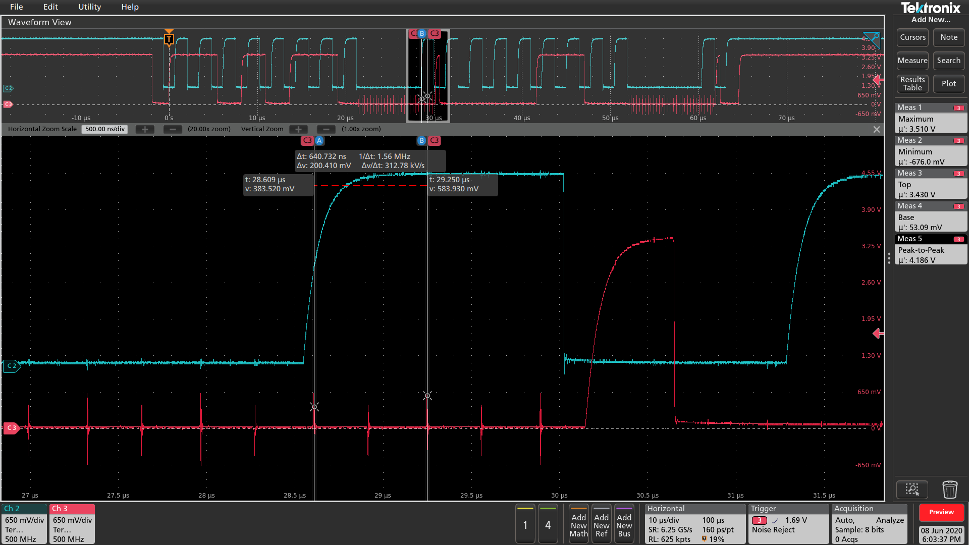
When using BQ25883, will find a switching nosie coupling into I2C SDA signal when the I2C finished 8 bits transmit and transmitter releases the SDA line to accept ACK signal. The SDA waveform is show as below (red for SDA, and blue for SCL).
The design is on a 6-layer board with 2 complete GND plane.
Can be seen that noise switching frequency about 1.56MHz, match boost switching frequency inside BQ25883.
Max negative voltage is about -900mV.
Could you please help analysis
1. the possible course of the problem
2. possible ways to solve the problem
3. if cannot be solved, possible influence, for example, will -900mV damage other devices
You can email me at:
jayce-luo@ti.com