This thread has been locked.

If you have a related question, please click the "Ask a related question" button in the top right corner. The newly created question will be automatically linked to this question.

UCC28701: Mysterious dead band between OCV and OCC

Part Number: UCC28701

Hi,

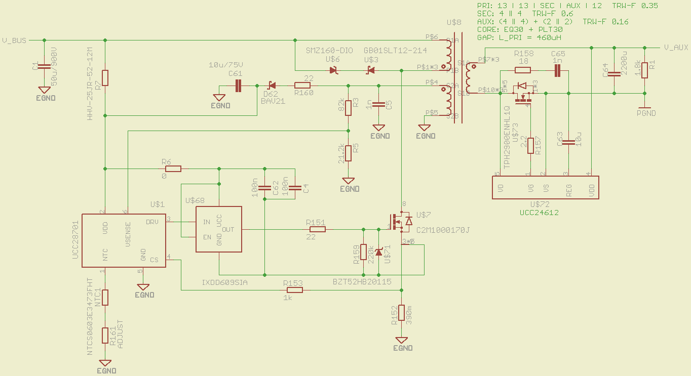
I am prototyping a 14V/4A flyback based on the UCC28701. It works mostly correctly, but I can observe the following mysterious behaviour:

1. At no load with 320V at the input, the converter enters the sequence of many cycles of restarts. It is ultimately terminated and 15.5V is present at output. If I decrease the dummy load resistor at the output to a value ~2 times smaller than calculated from the equations given in the datasheet, it starts in  a reliable way.

2. If I_out is smaller than about 3A, the output voltage is close to the desired value and rock-stable across the entire range.

3. If the load resistance is decreased to make I_out exceed the 3A limit, the controller enters the restart sequence again.

4. If the load is further decreased, the controller enters a stable region again and outputs ~9.5V at a constant current of 4.1A.

As described above, the transition between CV and CC is not smooth and the transition region where the controller refuses to operate is pretty wide. What might be the cause of this behaviour?

If you can also explain the hiccup mode in (1), it would be highly appreciated as well.

If more details are needed, just ask. Here are some:

L_pri=405uH, N_pri/N_sec=9.5 (38pri:4sec:6aux),

R_cs=350mOhm

R_lc=1k

R_s1 (top) =82k

R_s2 (bottom) =20k

V_in = 180..900V DC

V_in_run=117V DC

V_dd = ~20V

    Best regards, Piotr

  • Hello Piotr,


    Thank you for your interest in the UCC28701 flyback controller.


    For the “hiccup” restarts of symptom (1): each restart is a consequence of a previous shutdown. To solve this issue, we need to determine what is causing the shutdowns. The clues we have are that the restart attempts eventually succeed but the output voltage settles at 15.5V and that a higher minimum load starts up with no problem.


    I suggest that you follow this troubleshooting guide https://www.ti.com/lit/pdf/slua783 to track down what may be causing the start-up faults. One item to keep in mind is that MOSFET turn-off delay can allow higher Ipk than expected, given the low 405uH an high input voltage range. Higher Ipk delivers excess energy per cycle and may result in an overvoltage if the load is too low, and may also force the switching frequency to the minimum rate of 1kHz.

    Since excess Ipk from delay is proportional to bulk voltage, you may not have a start-up problem at voltages lower than 320V, but have trouble at voltages higher than 320V.


    If turn-off delay proves to be the culprit, then increasing Rlc will mitigate that. However, calculating the correct value of Rlc depends on an accurate assessment of the total delays from detecting the current at the turn-off threshold at the CS input to when the MOSFET drain voltage rises rapidly higher.


    For item (3): I suspect that switching noise is interfering with one of the control signals, causing a fault condition on which the controller is required to shut down. For load currents less than 3A, as in (2), the noise is not strong enough to interfere. For potential load currents greater than 4.1A, the CC limit of 4.1A is reached and the lower output voltage of 9.5V must mitigate the noise somehow. (I don’t know how.) For loads between 3A and 4.1A, the noise is strong enough to interfere.


    It can happen this way because each start-up is equivalent to starting into a short circuit. An output capacitor at 0V always gets charged with the full CC-limit current until Vout reaches regulation. Only then does the current delivery reduce to the steady-state load. With a resistive over-load on the output, Vout can rise to 9.5V and stay there in CC mode, until the load resistor is increased and Vout is allowed to rise higher. Apparently, higher voltage at the CC-limit then “succeeds” in interfering with a control signal.

    I don’t think it is noise at the CS input, but there is still a finite probability that the leading edge blanking is not long enough. If so, it is ironic that adding filtering at CS will also increase turn-off delay and exacerbate issue (1).

    The other possibility is a distorted signal on VS. But the signal should not be filtered. This pin detects critical timing information from the auxiliary voltage reflected from the secondary, so no capacitance should be placed on this node. However stray capacitance from the pcb layout may be present if care was not taken to avoid it.  

    It is not good to probe the VS pin with an oscilloscope probe, because that adds capacitance, too.   Only a low-C (< 2pF) active probe may be used. Otherwise, probe the Vaux and see if there is significant ringing during the demagnetization interval. Ringing may cause a false over-voltage to be detected, or clock in the wrong demag time to disrupt normal operation.


    Please follow up on these suggestions for debug.


    Regards,
    Ulrich

  • Hello Ulrich,

    Thank you very much for your extremely detailed answer!

    I will follow your pieces of advice. I had read the troubleshooting guide before I asked this question and sorted out the basic issues. Indeed, I had had some problems with the PCB layout, but these were subsequently fixed. The V_R_CS and V_DS waveforms look preety good now. I don't know what V_VS should look like, so I can't comment on that. I believe you are right with (1), there might be too much energy delivered from V_AUX. Lowering the dummy load resistor from 3.3k to 1.8k results in a reliable startup at 320V. I have updated my requirements and adjusted the prototype accordingly. For 46W/85% efficiency the component values were calculated by the attached Matlab/Octave script based on the datasheet equations. I believe the interesting part is below (engineering notation in SI units):

    f_max = 63e3 (limited by t_on_min, the driver/FET could go to hundreds of kHz)
    i_out =     3.4586e+000
    i_occ =     3.5000e+000
    v_ovp =    14.0000e+000
    v_occ =    12.0000e+000
    v_ocv =    13.3000e+000
    d_max =   512.0000e-003
    n_ps_max =    10.2138e+000
    n_ps =     9.5000e+000 (38:4)
    r_cs =   389.6357e-003 (used 390mOhm standard value)
    i_pp_max =     1.9231e+000 (the saturation current of the transformer is about 2.8A, so no issues here)
    l_p_max =   460.6815e-006 (calculated)
    l_p =   460.0000e-006 (measured)
    v_rev =   108.0368e+000
    v_dspk =     1.1311e+003
    t_on_min =   327.6353e-009 (the datasheet requires 300ns min.)
    t_dmag_min =     2.3246e-006 (the datasheet requires 1.1us)
    r_s1 =    83.9713e+003
    r_s1 =    82.0000e+003 (standard value)
    r_s2 =    19.9459e+003 (wrong, the 13.3V VOUT is at 21.2k).
    r_s2 =    21.2000e+003
    r_lc =     1.1008e+003 (used 1k, but the FET delay is unknown, assumed 50ns, to be measured exactly)
    iocc2 =     3.4967e+000 (based on the actual value of r_cs, not assumed)
    c_in_min =    44.6293e-006 (I have a 50uF/900V film cap)

    This converter is a startup power supply for a high-power LLC converter. It is also a secondary power supply for the entire system, feeding a power path prioritizer. It should chime in when the LLC unit is shut down, e.g. due to power saving mode or handling a short-circuit condition, etc. It is powered from the bulk capacitor of the PFC unit. The V_BULK (and hence the V_in of the flyback) is 600V under normal operating conditions, but it should start at the lowest voltage possible. 180V DC (128V AC 50Hz) seems to be a reasonable value for a heavy 230 mains Undervoltage, which the converter must still support. The 900V is a safety feature -- the converter should be operational within the absolute maximum ratings of the LLC unit. Low and high line efficiency is not a concern, the 500-700V range is where the converter will spend most of the time.

    Reliability is at a premium, so a SiC switch with a huge VDS margin has been used. Unfortunately, TI has selected the worst possible startup voltage of the UCC2870x family: the 21V (typ) 24V (max) is above the recommended V_GS of the switch (20V) and the 14V clamp on the DRV pin prevents the FET showing its full capabilities. So there is the IXDD609 to handle this issue. The number of turns of the auxiliary winding is designed to put the VDD of the controller in the 18-20V range with a Zener protecting the gate. The 9A capabilities of the IXDD609 are not utilised, it just happens to have idle current comparable to the UCC28701 (1uA typ, 10uA max), which allows for a large HV resistor value, i.e. low losses there. The UCC25731 initially planned there failed miserably, as it requires ~200uA.

    Below is a diagram of the prototype.

    Please mind the transformer is a planar unit, so the windings are lateral. Description: "||" means "bifilar", "+" means "next in the same layer", "|" means "next layer".

    The secondary-side snubber RC values have not been optimally selected yet, but they seem not to have any impact on the UCC28701. The secondary-side synchronous rectifier does not have any significant impact on the behaviour of the PSR controller, verified that with a Schottky diode. The calculated Vor is 13.3*9.5=126V, so I am not sure if the 160V Zener is high enough, but the drain voltage of the main switch looks beautiful then. The 1700V switch allows for a plenty of headroom, so if replaced with two 160V diodes, the ringing is substantially larger, but the PSR seems not to notice that. When running at 40W with V_in=320V, the prototype is barely slightly warm when touched: the temperature increase of the main components is so insignificant that there is no point in measuring it exactly. I am very happy with the results, so I only need to ensure that the UC28701 feels comfortable in this setup.

    Oscilloscope waveforms are available on demand.

        Best regards, Piotr

  • Hello Piotr,


    Thank you for all of the additional information.


    I have some observations for you:

    1. Your output OVP target of 14V cannot be met. The internal OVP threshold is 4.6V (at the VS pin) which is 0.55V or +13.6% of the reference voltage of 4.05V. For a 13.3-V nominal output setting, the OVP level will be ~15.1V.

    2. Your 50-ns estimate for MOSFET delay may be optimistic. Typical Si MOSFET delays run 100~200ns, depending on the Coss. I’m not sure what the SiC delay will be; you’ll have to measure it. However, be sure to also add in the propagation delay of your gate driver. Adjust R153 value to account for it as necessary.

    3. A single 160-V TVS clamp should be sufficient, especially if you are happy with the waveform.

    4. There is a 1-nf C5 across the Aux winding. I think the IC development engineer placed it there in an early design to abate some EMI noise, but normally we don’t put a cap across the Aux. I suggest to remove it and see if things improve, stay the same, or worsen. If it is needed, start with a lower value and work up to the necessary value.

    5. The VS waveform should look very much like the positive half of Figure 13 (or Figure 14) in the UCC28701 datasheet. The negative half is clamped to -0.25V by an internal circuit. Those figures show the Aux voltage, but VS would be scaled down by R3 and R5, and negative is clipped.

      From reading your last message, it appears that the increased minimum load has solved your problems. If that is the case, good luck with move to production. If I am misreading it, please send another post with a succinct issue.

      Regards,
      Ulrich

  • Hello Ulrich,

    Once again, thank you, your comments are very much appreciated. Just for the sake of completeness:

    1. Excellent spot, thank you. Fortunately, this is not a problem.

    2. I have just measured that with a scope: the time between the beginning of the falling edge of the DRV signal and the rising edge on the drain is 56.8ns. That includes the driver delay. The datasheet says to add 50ns of the internal controller delays to that value. OTOH, according to the scope, it takes 8.4ns for the MOSFET to turn off, which is fully consistent with the 10.8ns turn-off delay value from the datasheet. This transistor is blazing fast. Maybe even too fast...

    4. I added the capacitor as a troubleshooting control to mimic one of your EVBs, but it seems not to have any obvious impact on the behaviour of the controller. The reported problems referred to the situation without the capacitor.

    The increased minimum load has solved both the hiccup startup and the 15V overvoltage at no load.

    Would you be so kind to pass a request to your design teams to consider a PSR controller very much like the UCC28701, but able to drive a SiC switch directly? What you need to change is barely the gate driver stage (stronger and clamped to 20V, not 14V), the rest works correctly, as it has been proven by my application.

    Best regards, Piotr