This thread has been locked.

If you have a related question, please click the "Ask a related question" button in the top right corner. The newly created question will be automatically linked to this question.

LM5060: IC Failure when OVP trips > 60V

Part Number: LM5060

We have a board that closely replicates the LM5060EVAL design.

We have the OVP slightly higher, at 62V.  When we raise the voltage up to this threshold the LM5060 properly trips and shuts off the FET.  But then it proceeds to let its smoke out... Visible destruction of pin 2 (VIN).

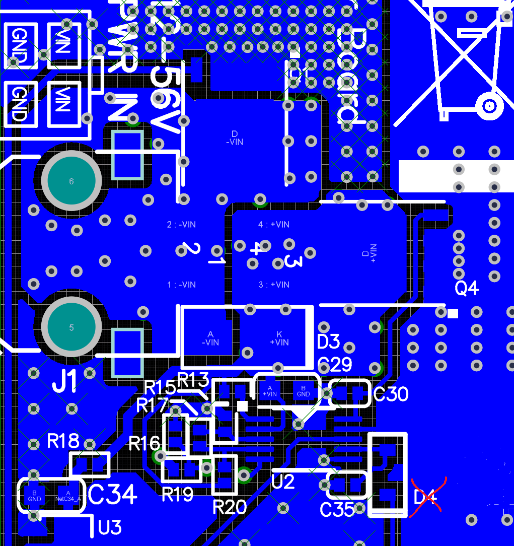
We have tried many many things, but are at a loss as to what is going on here.  This is a snip of our schematic:

We have done through dozens of LM5060's trying to get this figured out.  The issue appears to be worse with a load, though this is not required.  We have scope captures of the +VIN and +VMAIN when the OV trip occurs and the inductive kick is only a couple volts.  Another possible clue is that the nPGD signal (with 100K pullup to 12V) goes to the gate of a 2N7002 FET, and this FET is often damaged after the failure.  Perhaps a higher voltage escapes nPGD when the LM5060 fails?

But the weirdest observation is also the most repeatable: A brand new board blows on the first try when +VIN is raised to 63V.  Then we replace the LM5060, and the board is forever good.  The new LM5060 always works properly and never fails again.  We can't come up with an explanation for this observation, but it has been repeated many times.  Does this make any sense?

Thanks!

  • Hi Jason,

    Sorry to hear this. Can you help with full schematic (is there any additional output capacitance other than what shown above), layout. Also, share a test waveform of Vin, Vout, GATE, nPGD during OVP event. Please capture with reference to LM5060 device ground.

    Best Regards, Rakesh

  • Rakesh,

    Here is a bit larger schematic - I'm not sure I can publicly share the DC/DC buck converter design that this feeds, so I have removed that from this sch, but I did leave the 8x 10uF 1210 ceramic caps that serve as input caps for that converter - which are then also output caps on the LM5060 circuit.  This also shows the nPGD connection to the 2N7002 FET, and the 100K pullup to +12V.

  • Rakesh,

    Here is a snip of the layout:

    We realize this doesn't have the grounding done properly as indicated in the datasheet recommended layout.  There are several separate GND vias into the GND plane.  We did try lifting the GND side of C8 (VIN) and wiring that to GND at C35, to ensure the VIN bypass cap was referenced to the same GND point as the IC, but this did not change any behavior.  Could this layout difference explain the failures?

    Note that D4 as shown in the layout is not loaded (connected to the TIMER pin).

  • This is the VIN when the overvoltage trips - The Probes are AC coupled, but the DC offset is 62V at the trip point.  The yellow is the raw +VIN to GND and the magenta is at the input snubber cap (filtered by 1-ohm resistor).  

    I'll work on getting your other requested captures, but does any of this give you any ideas?  Thanks!

  • Hi Jason,

    Thanks for the details. The kick-back voltage on Vin during turn-off still looks under the abs max rating of the device. one reason, I can think of stressing the device during OVP event with output capacitance is the discharge path from OUT to the GATE through the clamping diode described in section "8.2.1.2.9 Large Load Capacitance" of the datasheet. But, it is not correlating with the Vin pin failure you observed.

    Can you share those captures, If there isn't any anomaly we can plan to get your board and units for debug and FA process. 

    Best Regards, Rakesh

  • Rakesh,

    This is a capture of the OVP event.

    • Yellow: +VIN
    • Magenta: VOUT
    • Blue: GATE
    • Green: nPGD

    Everything seems to look good here.

  • Rakesh,

    We pursued your comment about the output capacitance discharge path, even though as you said it doesn't correlate with the VIN pin failure.

    We first simply removed the two large 180uF electrolytics - and no more failures on OVP.  We reinstalled the two electrolytics and it failed on the first OVP trip.  So this does seem to be it.  80mA discharge at 62V is 5W of heat, a lot, and with Cout = ~400uF the duration is long, linear drop over ~300ms.  This is nearly 1J of energy, likely way too much for the IC package.  

    The datasheet recommends adding a series R to VOUT to address this, but we do not want to do that as this would result in the VGS being exceeded, and damages the FET - The gate will get pulled way below the drain, much more than the +/-20V max.  I feel like the suggestion in the datasheet is not a safe solution.

    Instead we plan to remove both electrolytics after the FET, but install one of them before the FET - our testing indicates that only one is needed anyway.  This seems to be a good solution moving forward.  

    Thanks for your suggestion on the output capacitance discharge path!

    Jason