This thread has been locked.

If you have a related question, please click the "Ask a related question" button in the top right corner. The newly created question will be automatically linked to this question.

TPS61022: Noise output from the Inductor.

Part Number: TPS61022
Other Parts Discussed in Thread: TPS61023, TPS61253A

Hi, i have a problem with the noise produced by the Inductor of the boost. Its audible and affect on the Audio output of the circuit.

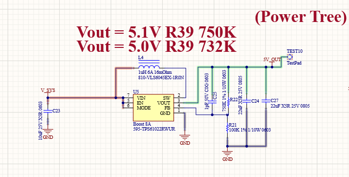
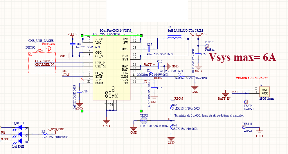
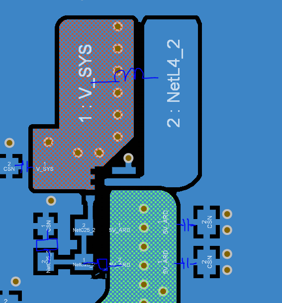
Note: the 1pf capacitor on the feedback resistors its not soldered, C25 on the schematic.

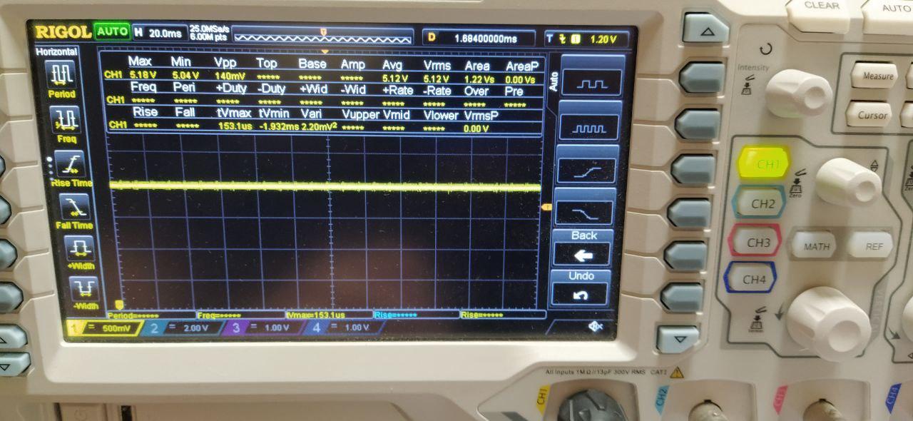
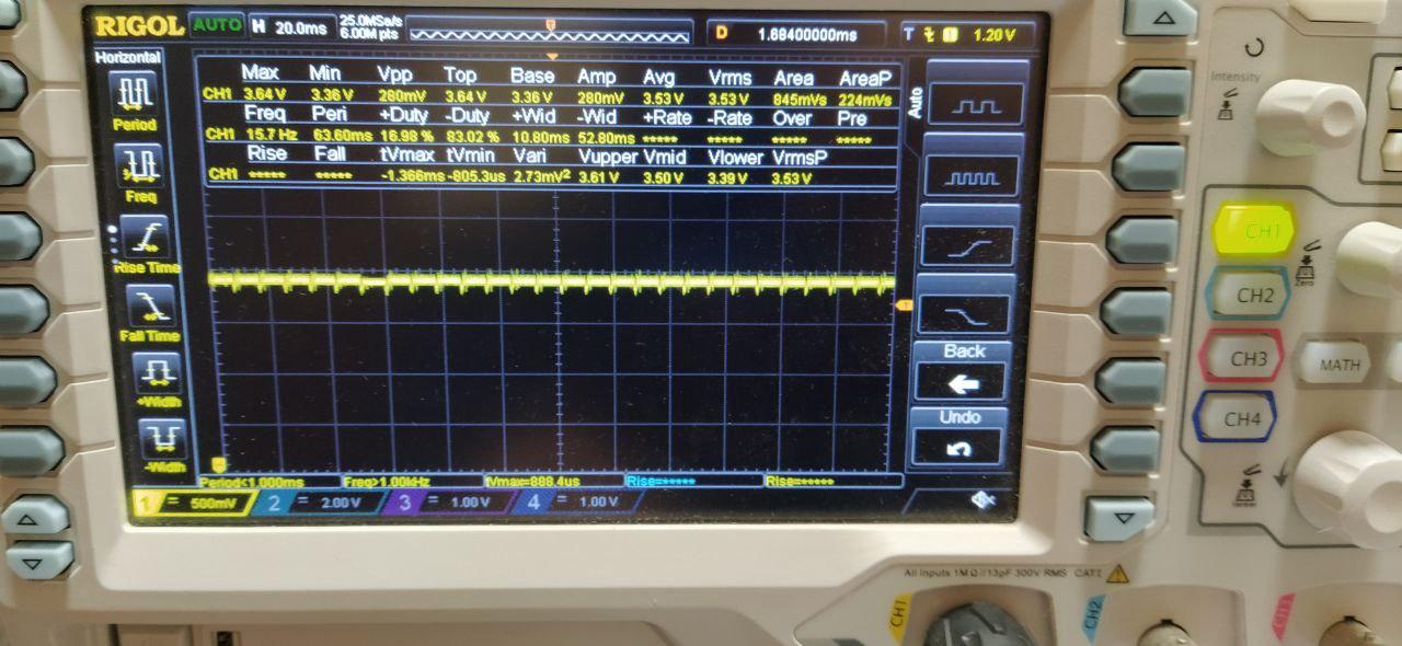
This its my circuit at this moment, as you see i force the mode to PWM to solve about 60% of the problem, but when the input reaches low voltages near to 3V (its a Lipo 1 CELL the battery input of the circuit) it starts to emite audible Noise.

The charge of the circuit its a computer module 3 from raspberry pi, so we will have a minimum load of 0,5A on the 5V lane, and a maximum of 3A. In theory the datasheet sais thad from a LiPo battery this integrated can offer 0 to 3A without any problem, and it works really good, but the problem for me its the inductor.

It's my inductor a bad choise maybe?, its a VLS6045EX-1R0N, and following the specification of the datasheet it should be valid for the design.... or i am wrogn?

The parameters of the Inductor are as follows:

Part Status Active
Type Wirewound
Material - Core Ferrite
Inductance 1µH
Tolerance ±30%
Current Rating (Amps) 6A
Current - Saturation 12A
Shielding Shielded
DC Resistance (DCR) 16mOhm Max

Any help would be appreciated, regards Carlos.

  • Hi Carlosp,

    please try to increase output capacitor. It could be caused by the stability. also measure the VIN and VOUT waveform.

  • Hi Jasper, i will test today with a higher Ceramic capacitor out, at this moment it have 2x 22Uf and one 22Uf extra capacitor.

    One question, should we solder a Feedback capacitor?, at this moment its unfited.... but the datasheet and the Excel recomend to introduce one. In our practices this capacitor create some noise and unstability, but could be a problem from our side.

    Regards, Carlos..

  • Hi Carlos,

    1. The selected inductor VLS6045EX-1R0N saturation current 12A is high enough but the Itemp spec 6A is quite marginal. When output power is 5V*3A=15W, assume the efficiency is 92%, the average input current is 15W/0.92/3.0V=5.43A. The inductor temperature rise is around 30-40 degree but it's ok as it only works at 3.0V Vin for very short time. And it should be not to root cause of audible noise.

    2. The feedback capacitor is not necessary. It is only needed when you want to optimize the loop response speed.

    3. Can you share the layout and probe the SW pin waveform. The device is working at FPWM as you connect MODE pin to Vin so I'm quite curious why you can still hear audible noise.

  • I am on the lab working on the tests, i gonna back this week with more information and results.

    Thanks for your help.

  • Attached the images of the otputs. It seems to be OK and without any problem. The noise get sync with the Processor Noise of the computer module3 from raspberry, and now its really really low, you need to put the ear over the inductor to hear that.

    Kinda strange, its the first time something like that happend to one of my desings. The charger its from TI too, its a BQ25606RGER.

    Then the L2 its a GND plain.

    As the product will be closed, on this relase we will accept that noise as normal, but in the next review we should correct it, maybe selecting another Boost from texas instrument with a higher frecuency.

  • Hello Carlos,

    You could check if the noise further reduces by changing to a physically smaller inductor.

    Another audible noise source could be the ceramic capacitors. To be 100% sure, I recommend to check if the noise is gone when you remove the inductor and connect it through wires. Normally the board needs to amplify the inductor oscillation to hear it.

    If the noise is still there, you might be able to reduce it by replacing the output caps with special ones that reduce audible noise.

    Audible noise is normally amplified through the board, so sometimes it helps to place the converter to the edge of the board. In addition I would recommend to not use thermals for the capacitors.

    As the converter is operating in PWM, I expect that the noise is caused by the load, not the switching frequency.

  • Hi Carlo,

    Besides Brigittes's suggestions, you can also probe the SW pin waveform. We cannot tell if the loop is stable or not by only watching at VOUT pin waveform because it only shows up the DC level. If you see the SW pulse width unfixed, it proves the noise comes from inductor. If the pules width and duty cycle are quite fixed, the noise may come from other part on the board.

    I see the layout of your board is not good. The output capacitors are not placed close to IC VOUT and GND pins on top layer. We used to see the device failure cases with similar layout on E2E. Please update the layout per AN: SLVAES4

  • Thanks Brigittes/Zack. Well noted about the layout design, so i was doing it wrong in a lot of buck/boost designs, i will change my designs in order to fit those APP guidelines.

    First capacitors, then i can routed the Feedback lane.

    I will try to look for some inductor that can fit on the footprint on the board, any sugestion?, and test to solder it throuhg wires. Maybe the noise comes from the broadcom CPU of the raspberry itselfs.... when i run the stress tests i could appreciate how the noise gets sync with the CPU load, but if i use a lab power supply instead of the Boost i cant hear any noise.

    Regards, Carlos.

  • Hi Carlos,

    XEL4030-102MEC is one choice. Let me know once you have test results.

  • In the following weeks i gonna recive a new design, i introduce the changes of the capacitors into the layout.

    After test of working we see a max comsuption of 1,4A at 3,10V. So this booster its really over the needs i think, or should i change it?. At this moment on the test without think on the noise its working really well.

    Regards, Carlos.

  • Hi Carlos,

    You used to say: The charge of the circuit its a computer module 3 from raspberry pi, so we will have a minimum load of 0,5A on the 5V lane, and a maximum of 3A. So the input current should be really high.

    Does the raspberry pi draw 3A from the TPS61022 output when you see a max comsuption of 1.4A at 3.10V Vin? 

  • Hi thanks for your answer.

    Actually under the normal use test and extress test we have:

    Normal use: 2.64Watt to 3.10Watt.Average input current is 2.64W/0.92/3.0V=0.95A || 3.10W/0.92/3.0V=1.12A

    Extress test: 5.69Watt to 6.12Watt. Average input current is 5.69W/0.92/3.0V=2.06A || 6.12W/0.92/3.0V=2.22A

    So no, the raspberry Pi never reach the draw point of 3A under the 5V output as their datahseet recommend.

  • Hi Carlos,

    Understood. If the maximum power is only 5.69W, I think TPS61023 is a better choice. Its current capability is about half of TPS61022.

    TPS61023 enters into PFM mode at light load and switching frequency reduces. If you still worries about the inductor audio noise, you can use TPS61253A.

  • Thanks Zack, i am on the final steps of the new revision, i gonna try this new boosters your recomend after read the datasheet.

    With this i can solve the issue, thanks for your help.