This thread has been locked.

If you have a related question, please click the "Ask a related question" button in the top right corner. The newly created question will be automatically linked to this question.

LM43601: Webench design not working as expected

Part Number: LM43601

Hello guys,

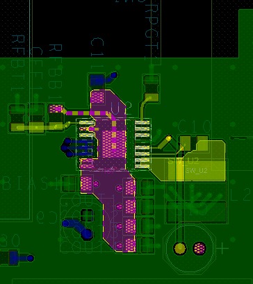
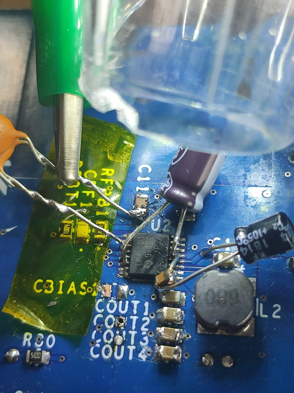
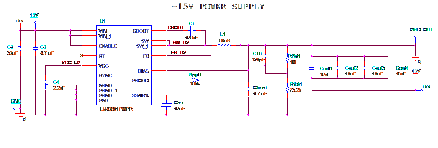
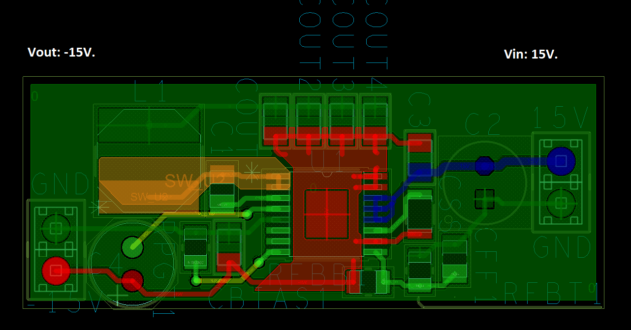
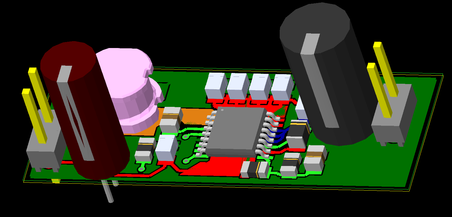
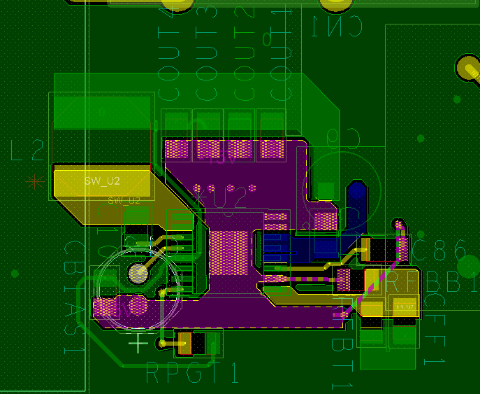
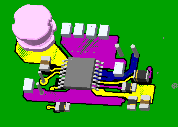
I have designed -15V Inverter design based on Webench simulation. But It's not working (0.67 V).

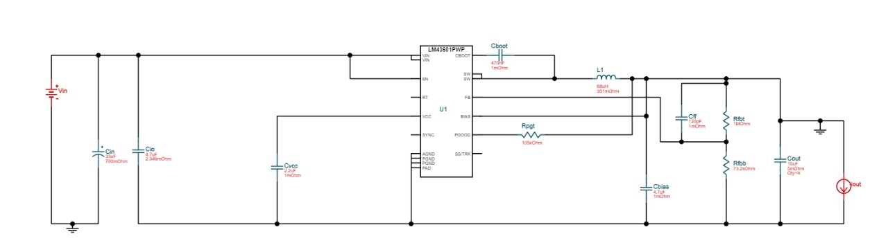
If I make a instant short circuit connection between V output and GND, it start working as it supposed to (-15V). What should I change from the Webench design?

Regards,

Pascal.

  • Hello Pascal,

    Can you try adding a 47nF SS cap from SS pin to -ve Vout and retry?  If this does not resolve the issue, please reopen the thread and please can you share your layout?

    Thanks, hope this helps?

  • Thanks for the suggestion, I will test it today and let you know!

  • I tried to put the 47 nF cap from SS pin to Vout and didn't work, I still have the same behavior.

    Here is the layout that your requested. Purple is -15V and blue 15V for your reference.

  • Hello Ernesto,

    It appears the layout is very different from the recommendations given in the Datasheet and I suspect that this could be the issue?  Switching converters require the following layout rules to be implemented in order to ensure reliable operation.

    Please review the layout guidelines in the datasheet and note the following placements.  Please consider these as critical for your design that require direct connection from component to pins with minimal impedance paths..

    1. Input capacitor placement that goes from Vin to Pgnd pins

    2. Boost capacitor between boot pin and SW pins

    3. VCC and Bias capacitors need to be placed from their respective pins and Pgnd.

    4. Feedback resistor placement close to IC pins

    It looks like the 2 and 4 are acceptable in the above layout, but maybe able to improve on a layout revision if indeed this is the case?  1 and 3 appears to be in violation of the rules I stated above?

    Suggest you kludge in these recommendations to ensure you can get this design working before embarking on a layout revision.  

    Hope this helps?

  • We made the recommended modifications and we still have a Vout of 0.63V. When we make an instant short cut between GND and Vout it start working at -15V, so same behavior.

    Here is a picture of the circuit with the kludge modification:


  • Hello Ernesto,

    Thanks for sharing the photo. Unfortunately you need to use good quality ceramics with low ESR for Cin and Cout.  Also, the way the capacitors have been kludged in is not ideal, you have long leads etc.

    Make sure you are using the the same inductor or equivalent that WEBENCH recommended.  Also I would scrape resist from the top surface to expose copper and solder down ground connect there to ensure short return path for the VCC and Vbias caps.  At some point you may need to take a risk to spin the board due to layout being far from ideal to eliminate this as being the issue.  If you do decide to, please post new layout and we will review for you before you send out to minimize risk of layout issues and problems.

    Hope this helps?

  • Hello David, 

    Here is update following recommendations:

    Schematic:

    Layout:

    3D drawing:

    The next step shall be fabricate, but we would like to confirm with you before and be sure it will give -15V out.

  • Hello Ernesto,

    A few comments on your schematic:

    1. Ensure that input and output traces are as wide as possible, this will reduce any voltage drop across the trace due to current flow. Consider using copper pours instead.
    2. Avoid sharp angles like those seen in the -15V trace.
    3. Place the output capacitors close to the Vout end of the inductor and closely grounded to the PGND and exposed PAD. 

    Hopefully this helps.

    Kind Regards,

    Harrison Overturf

  • Hello Ernesto,

    I believe this issue is resolved.  If you're still having issues, feel free to reopen the thread.  Thanks!

    Kind Regards,

    Harrison Overturf

  • Hello Harrison,

    Here is our update in layout...

    3D view:

    Any comments please let us know or if it's good to go and manufacture.

    Best regards,

    Hector.

  • Hello Harrison,

    Could you confirm with the layout redesign so we can continue with the PCB manufacture?

    Regards,

    Pascal.

  • Hello Harrison,

    We made the suggested changes to the layout design, could you confirm that the new design is suitable to manufacture?

  • Hello Hector,

    It's hard to tell from your layout whether or not you have connected a SYNC pin to GND. This SYNC pin should not be left floating, please ensure this is connected to GND.

    Otherwise looks good. Let me know if you have additional problems or questions.

    Regards,

    Harrison Overturf