This thread has been locked.

If you have a related question, please click the "Ask a related question" button in the top right corner. The newly created question will be automatically linked to this question.

LM27762: inquiries regarding supply

Part Number: LM27762

Hi team,

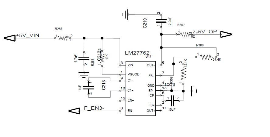
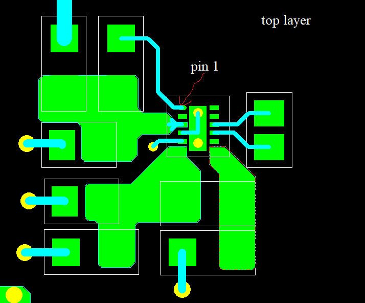
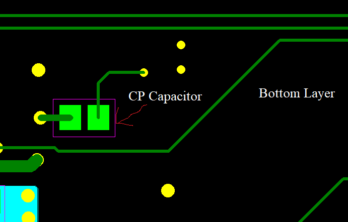
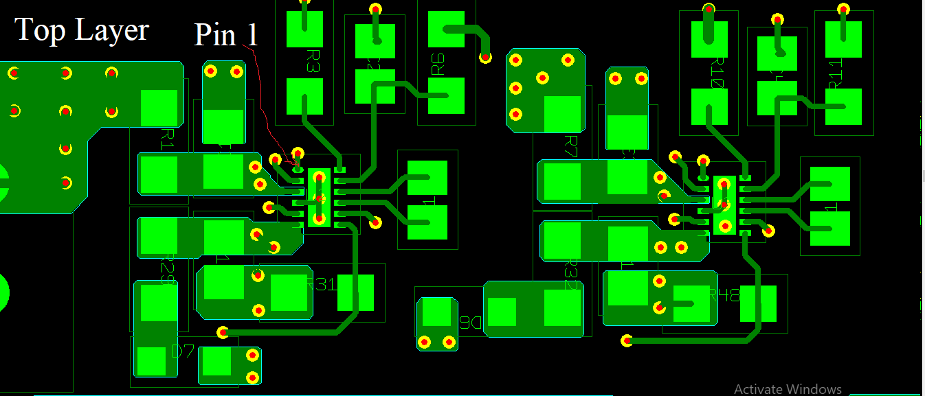
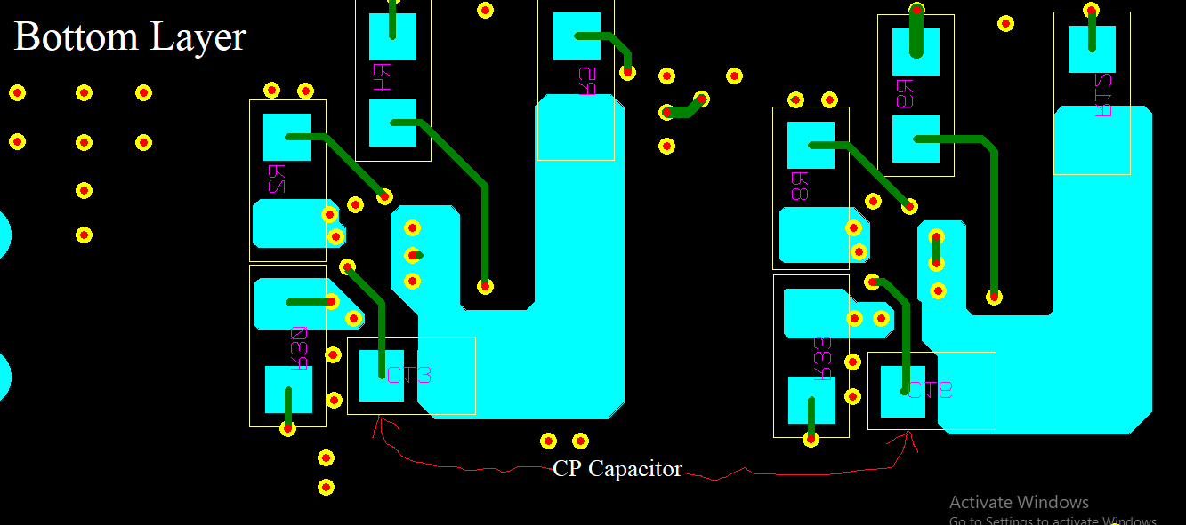
I am using the LM27762 power module for the generation of -5V supply from 5.5V input.

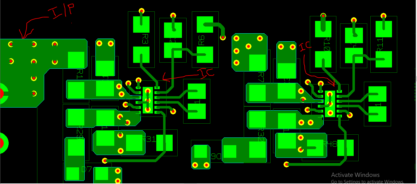
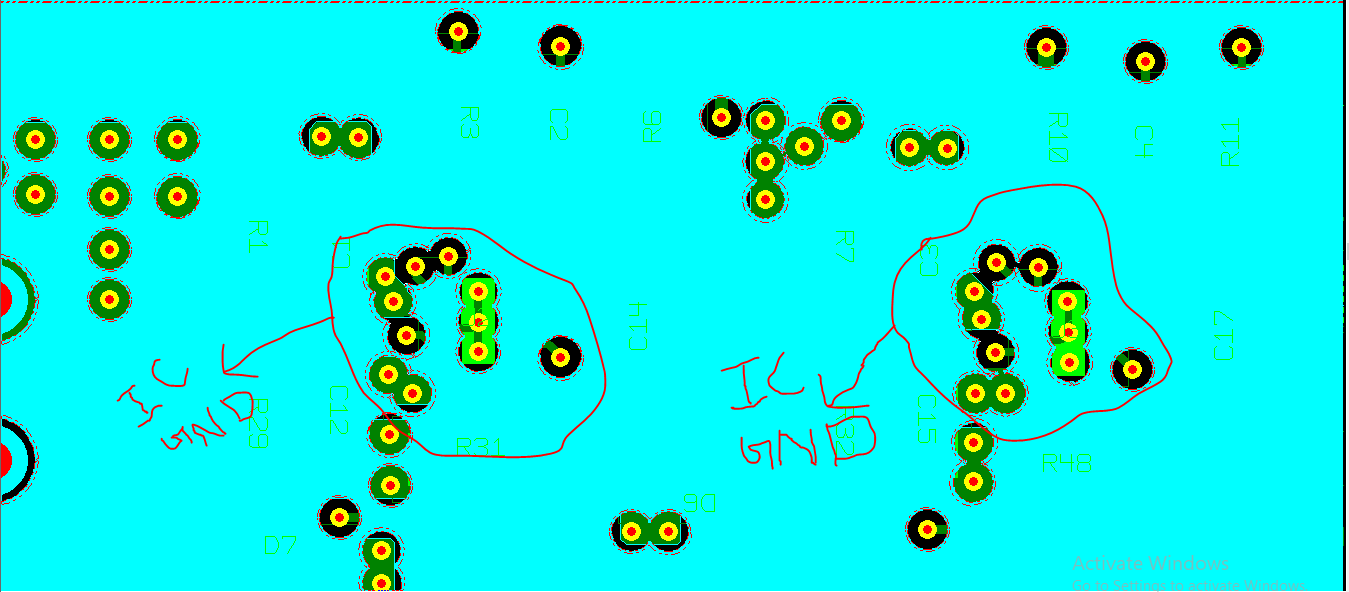
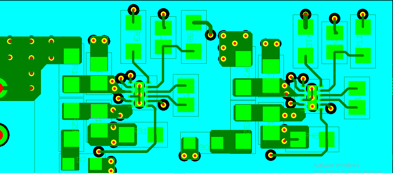
and I am using both the same module in a parallel connection to get more O/P current but I am not getting -5V O/P.

Initially, I am getting 0.4V of O/P when both the diode D6 and D7 are connected. But when I removed 1 diode both of them the voltage remain the same.

But whenever I removed both the diode D6 and D7 I am getting -2.35V  O/P of both the module separately.

Please review my design & Let me know where I am doing wrong.

  • Hi Ashish,

    Looking at the schematic, I see that you have used a 51kOhm resistor for R2 and R4 and a 238kOhm resistor for R1 and R3. Replacing the values of R3 and R4 into equation 3 from the datasheet for the LM27762 results in a set Vout of -6.91V which is not the -5V of output you are targeting, moreover it is outside the capabilities of the LM27762.

    Regards,

    Davor

  • Thanks for the quick reply,

    I know that thing and already change the resistor.

    now I am using 78.7KOhm  resistor for R2 and R4 and 240KOhm resistor for R1 and R3.

    As per the calculation, I should get -4.95V on the O/P but still, I am getting -2.3V on O/P of both the module separately.

  • Hi Ashish,

    Do you need the positive output for your application? Because it looks like you are not using it, but it is still enabled.

    If you just need a voltage inverter, then I could recommend a better solution LM27761 (which only has the negative VOUT).

    Regards,

    Davor

  • Hi 

    Thanks for the new ic suggestion.

    but I want to tell you I removed all the resistors and capacitors from positive O/P.

    I m using this module in my other design with the only negative O/P and it is working fine.

    I am getting O/P as per the calculation. So I don't think there is any issue.

    Please review my other design and let me know.

    In this design R1 is 140KOhm and R2 is 51KOhm so as per the calculation I should get -4.56V and I m getting -4.55V.

    So I can't understand where I m wrong and where the issue in my circuit.

  • Hi Team,

    I am waiting for your reply.

  • Hi Ashish,

    The new schematic you have sent doesn't have the diode at the output and also the resistors at the feedback divider do not have the values you mentioned in the previous message. R2 of 37.4 kOhms is not recommended as per the datasheet (the minimum recommended value of R2 is 50kOhms). Does your circuit still contains the diode at the output?

    Please send the most recent schematic and if you can also the most recent layout.

    Regards,

    Davor

  • Hi Davor,

    I already mentioned to you in my previous reply that I am using R1 is 140KOhm and R2 is 51KOhm.

    So I think it is ok as per datasheet and my circuit is not contained the diode at the output.

    I am getting 2.3V output from both modules separately and there is no diode connected om the output.

    I hope you got my point. What is I am saying about? 

  • Hi Ashish,

    Can you confirm that you are using low ESR ceramic capacitors?

    And what is the load of your application (Iout)?

    Also if you can please send the layout to be reviewed as well.

    Regards,

    Davor

  • Hi Davor,

    yes, I am using low ESR ceramic capacitors around 15 to 20 mOhms.

    The load of my application is around 300mA.

    Please review my layout.    


  • Hi Davor,

    yes, I am using low ESR ceramic capacitors around 15 to 20 mOhms.

    The load of my application is around 300mA.

    Please review my layout.    


  • Hi Ashish,

    I have looked at the PCB layout and I have several suggestions to make:

    1. Ccpout should be placed on the top layer (same layer as the LM27762) and as close as possible to the VOUT and GND pins. The returns for both CIN and CCPOUT must come together at one point, as close as possible to the GND pin. 

    2. Wider and shorter traces should be used for the flying capacitor C1 (it should be placed closer to the IC)

    3.R3 and R4 should be as close as possible to the FB pin and for best performance R4 should connect back to the GND connection at the thermal pad of the device. 

    4. Avoid using too many vias since they add to the parasitic inductance

    These suggestions are also listed in the datasheet for the LM27762 on page 17 and 18. Also you could have a look at the layout of the LM27762 EVM shown on page 10 of the EVM user guide.

    Again I will note that the last schematic you have sent differs from the layout, I am assuming that the resistors that would connect to the EN+, FB+ pins and the capacitor that connects VOUT+ to GND have been removed from the test board?

    Regards,

    Davor

  • Hi Davor,

    Thanks for the layout suggestion.

    But my layout is done and my manufacturing and assembly are also done.

    right now I am testing my board and facing this type of issue.

    So I can't do anything in my layout as suggested by you.

    The last schematic which I sent to you that was my other board schematic where I am getting proper output as per the calculation and the layout which I sent to you is my current board schematic where I am not getting proper output.

    Yes, the resistors that are connected to the EN+, FB+ pins, and the capacitor that connected VOUT+ to GND is removed from my board.

    The only difference in my working board and non-working board is that,

    I am using 2 modules parallelly both are connected with the diode and connected positive circuit but as I mentioned you I removed both the diode and resistors, capacitors from the positive circuit of the modules.

    But after did all these things I am not getting proper output as per the calculation.

    so, please let me know what should I do to get proper output.

    Regards,

    Ashish


  • Hi Ashish,

    Confirm if I understand correctly. You have another board where the LM27762 is used to give an output only on the negative rail with the same layout as you have given me. But the problem arises when you are trying to use 2xLM27762 in parallel with the same layout and schematic? 

    Regards,

    Davor

  • Hi Davor,

    Yes, you are saying correctly.

    Now you got the my point. 

  • Hi Ashish,

    I have a proposal, could you check if each charge-pump is regulating the output separately on this board (not your other design containing one LM27762). Just use a lower current load than the 0.25A limit and isolate the other converter from the output. Do this test for both converters, so that we could be sure they can regulate the output on their own and the issue occurs only when they are connected together at the output.

    Regards,

    Davor

  • Hi Davor,

    Thanks to you for this proposal.

    But I already did these things with my circuit. I have connected load according to 50mA  and isolate other converter from the output.

    I also did these things with both the regulator separately. But after did all these things I am getting still 2.3V output.

  • Hi Ashish,

    Since the converters are not regulating the output voltage separately at the desired level, then of course they wouldn't manage to do it in parallel. I still believe that the layout could play a part in this.

    In any case, I am getting to the conclusion that the LM27762 is not designed with current sharing in mind. 

    Regards,

    Davor

  • Hi Davor,

    But in my case, I am getting output 2.3V on both the LDO.

    And your concern about the layout than it is playing a role in wrong output so I think it is not possible because I am disconnected both the module from parallel connection and in my current scenario they are isolated from each other.

    Please explain to me this thing. 

  • Hi Ashish,

    The layout could certainly be the issue with the board, as I was referring to the layout of your single LM27762 (not both of them together). Also like I mentioned before the LM27762 is not designed with current sharing in mind, so perhaps when you have run your tests at full load one of the charge-pumps might have drawn quite a large percentage of the total current and might have caused some damage thus in the following tests the other charge-pump might have had the same issue. 

    When they are isolated, check if the voltage of the CP pin on both converters - it should be close to VIN. Also please check that FB- is with in specs (-1.22V) on both converters. A faster approach would be to change the ICs with new ones if you have them on-hand and keep their outputs isolated performing the tests at a lower current so that we could check if they can regulate the output on their own.

    Regards,

    Davor

  • Hi Davor,

    I did as per your suggestion on both the module.

    The voltage of the CP pin on both the converter is 2.2V and FB- is 0.8V with no load condition and output is 2.3V

    When I loaded it with 100mA load the voltage of the CP pin on both the converter is 1.8V and FB- is 0.082V and the output is 0.230V.

    This is my observation of both the module separately.

    I also replace both the ic with the new one but after that, the output remain same.

  • Hi Ashish,

    Given your results, this seems like a layout problem to me. A particular issue with your layout is the placement of the Charge-Pump Output Capacitor (as far as i can see it is not even in the picture of the layout you sent), which according to the datasheet should be placed as close to the IC as possible and on the same layer as the IC. Like I posted before, I saw some other issues with the layout and more information on how to do a proper layout of the LM27762 can be found on page 17 of the datasheet.

    In any case, for your application that has an output current larger than the limit of the LM27762 I suggest not using this device in a current sharing configuration. What I could suggest is to use a buck converter in an inverting configuration just like our reference design: https://www.ti.com/tool/TIDA-01457. This will result in a easier layout and design, only 1 IC instead of 2 and also it uses significantly less external passive components.

    Regards,

    Davor

  • Hi Davor,

    As you are saying about that may be problem in my layout and as per the datasheet recommendation the CP capacitor place as close as possible to the ic and same layer.

    But my concern is that in my working board where I am getting proper output as per the calculation I also did the same layout.

    Here I am attaching my both working and non-working board layout.

    Please review this and let me know where I am doing wrong.

    Working Board Layout

    Non-working board layout

  • Hi Ashish,

    First of all, there are differences between the two layouts you have sent, I will just point out a few of the obvious ones:

    1. R3 and R4 are much closer to the IC and one of them is not routed through a via like in your non-working board
    2. The trace for Vout is larger on your working board
    3. The trace for FB- is larger on your working board

    There are some other differences but basically you are comparing 2 different layouts here. In any case our recommendations about the layout will always be according to the datasheet which I linked previously, that is why I will still say that placing the CP capacitor on the same layer with the IC is the better choice and following all other recommendations in the layout section of the datasheet (on page 17), as much as possible, is the best way forward for your design.

    I will also repeat the same thing I mentioned in the previous reply. The LM27762 is not designed with current sharing in mind, so a much better option would be for you to consider the reference design https://www.ti.com/tool/TIDA-01457 which is a buck converter in the inverting configuration.

    Regards,

    Davor