Because of the Thanksgiving holiday in the U.S., TI E2E™ design support forum responses may be delayed from November 25 through December 2. Thank you for your patience.

This thread has been locked.

If you have a related question, please click the "Ask a related question" button in the top right corner. The newly created question will be automatically linked to this question.

BQ25703A: BQ25703A MOS and inductance hot when in boost mode

Part Number: BQ25703A
Other Parts Discussed in Thread: CSD17551Q3A, CSD17551Q5A

Hi

My customer designed with BQ25703A. BQ25703A works in Boost Mode, input voltage 12V charges 4S1P LiFePo4 battery (maximum 14.6V),  registers setting as below:

Charge Option 0 820E
Charge Current Register 0800
Charge Voltage Register 3900
OTG Voltage Register 0000
OTG Current Register 0000
Input Voltage Register 2100
Minimum System Voltage 2D00
Input Current Register 3C00
Charge Status Register B400
Prochot Status Register 0040
Input Current Limit In Use 3C00
VBUS and PSYS Voltage Read Back 8410
Charge and Discharge Current Read Back 1E00
Input Current and CMPIN Voltage Read Back 3900
System and Battery Voltage Read Back B2B1
Manufacture ID and Device ID Read Back 7840
Device ID Read Back 1078
Charge Option 1 9210
Charge Option 2 02B7
Charge Option 3 0000
Prochot Option 0 4A54
Prochot Option 1 8128
ADC Option 2000

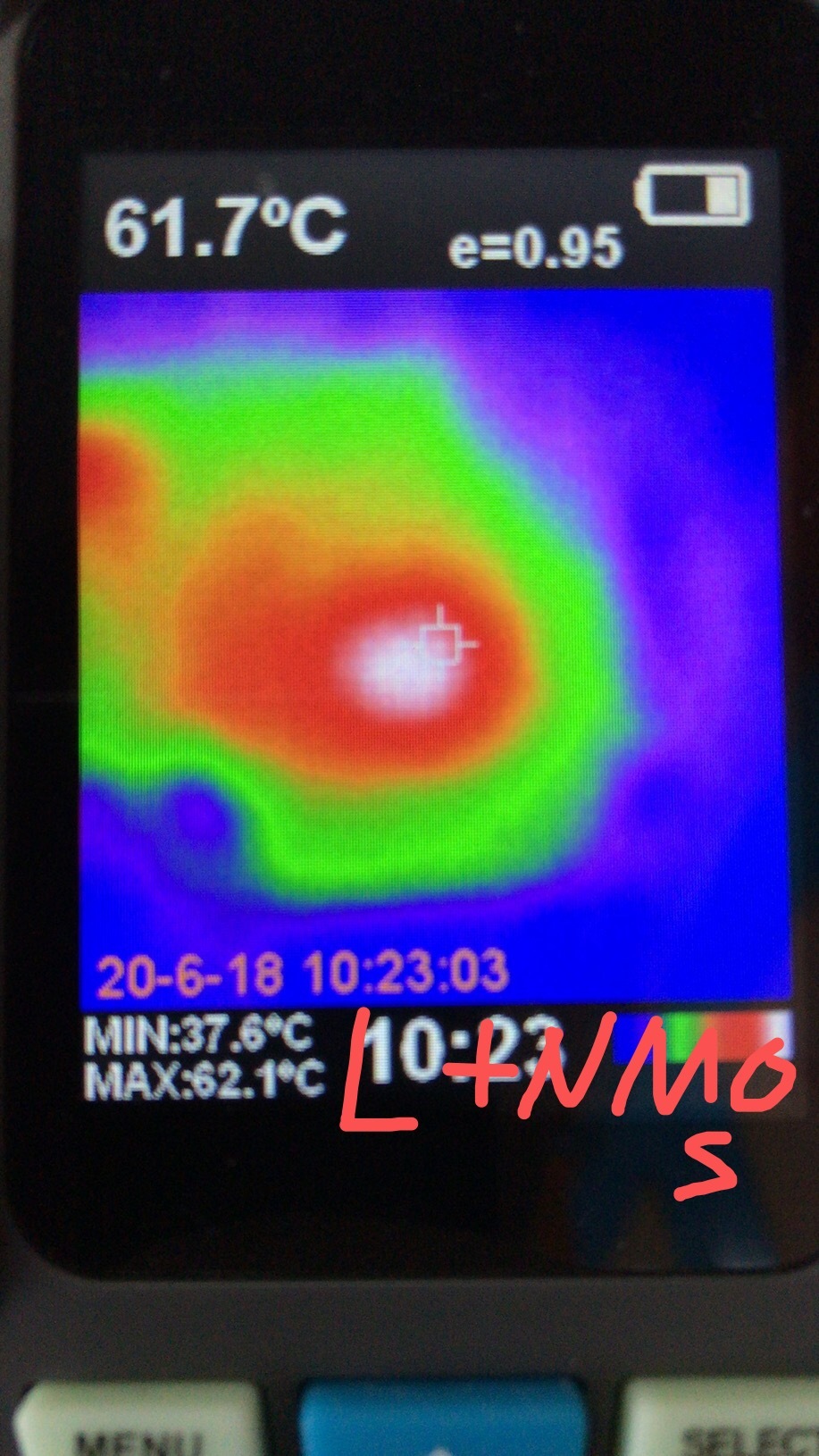
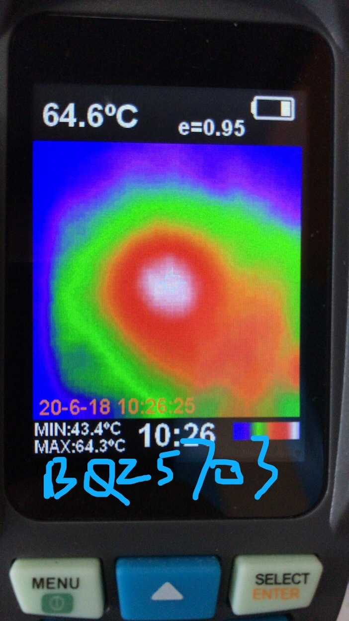
VIN=12V, VBUS=12V, VSYS&VBAT (the voltage slowly rises to 14.52V), the charging current is 2024mA, and find that the inductance (L1) and two MOS tubes (Q14&Q16) and BQ25703A chip in the boost mode are very hot, The larger the charging current configuration is, the hotter it is, when the charging current is 1024mA there is no problem.

NMOS tube selects NTMFS4833NT3G, RDS(ON)= 2.0mR@10V, Id(max)=191A, SO-8 FL package;

Inductance: 74437356022 2.2 μH, 8.5 A, 0.0203ohm;

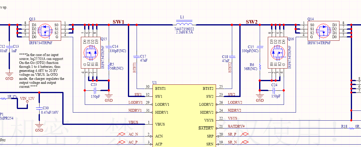
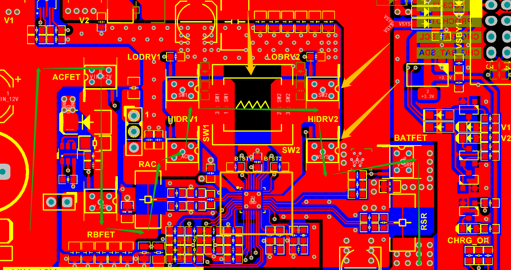
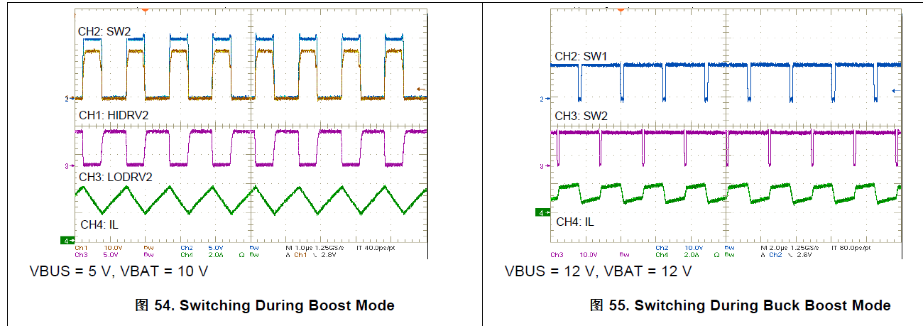
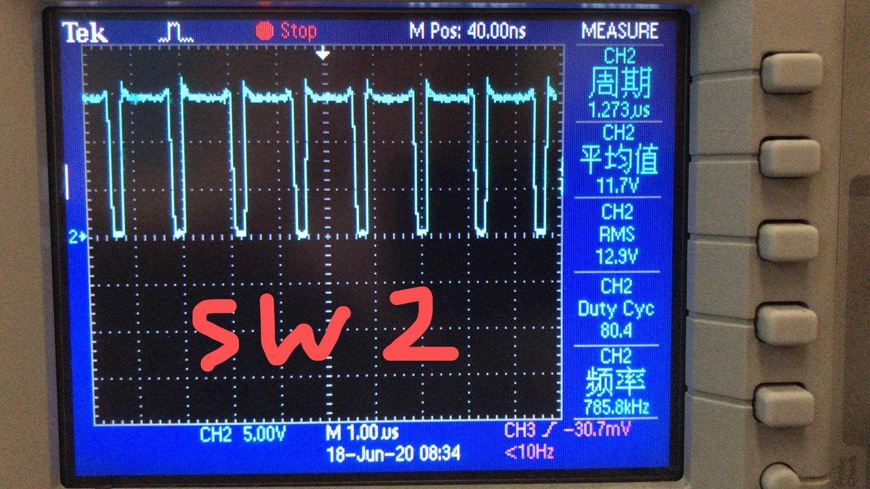
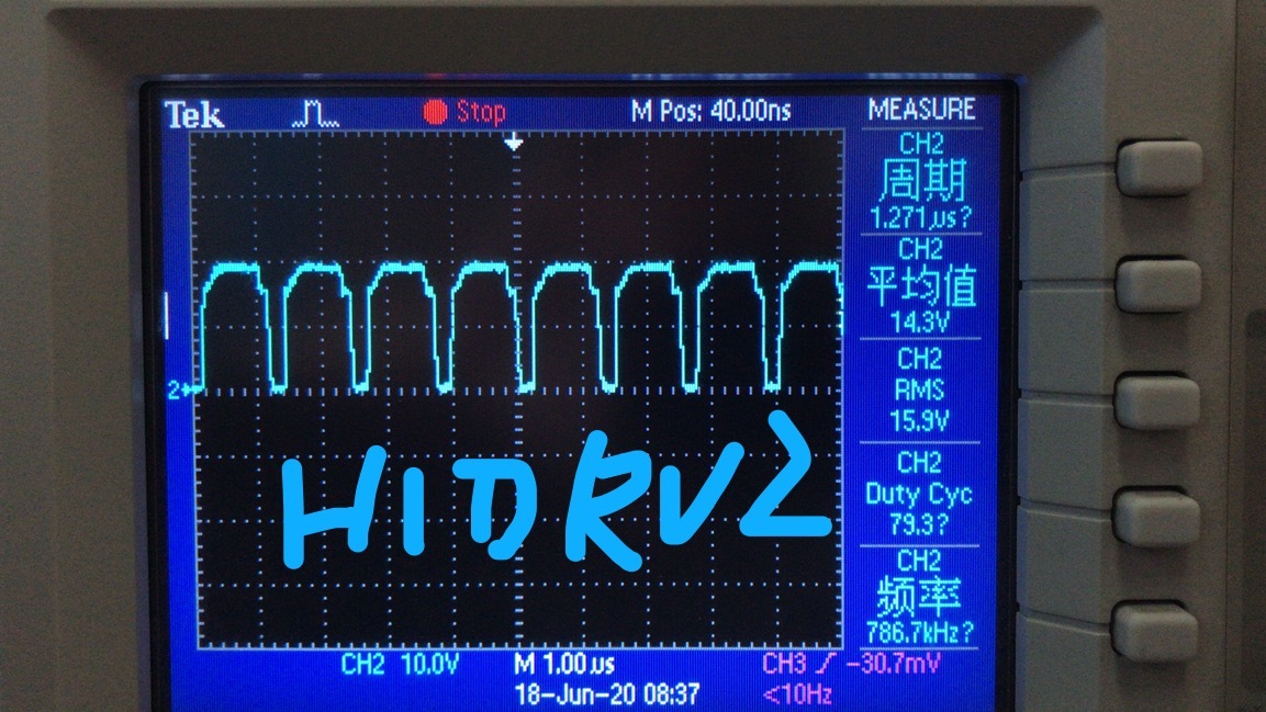
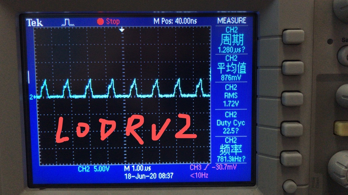
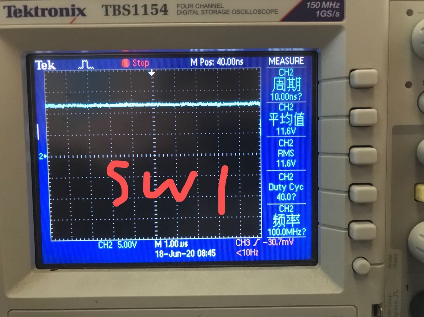
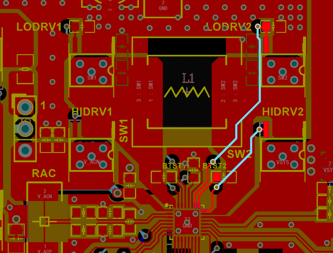
The following six pictures are SCH, PCB, signal waveform and heat map, please help check.

 Thanks

Star

  • Thanks for sharing your design information. 

    Your layout looks fine. The waveform HIDRV2 and LODRV2 is abnormal slow, which may result in high switching loss and high thermal dissipation. Suggest looking into the component value such as REGN cap, BTST2 cap, also the gate drive trace and resistance. 

  • Hi,Tiger Zhou,

    Thank you for your reply. I still charge 2048mA to charge the iron-lithium battery. The measured REGN voltage is 5.97V. The gate drive trace is as shown. The PCB board has four layers and the gate drive trace is on the third layer (1OZ) ,The measured resistance at both ends of the gate drive is 0.4~0.5 ohms. The oscilloscope looks at the waveform again to confirm that it is really abnormally slow. I don't know what measures can be taken to solve or improve these abnormalities?

  • We used to use wide trace for gate drive. You may try TI-FETs CSD17551Q3A since they have low gate capacitance. 

  • Hi Tiger Zhou,

    Because of the PCB packaging of materials, I chose the TI CSD17551Q5A model for testing. The parameters of the two are almost the same. Among them, the parameters: Qg=6.0nC, Ciss=1050pF.

    Regards,

    Huigen Jiang @F&R