This thread has been locked.

If you have a related question, please click the "Ask a related question" button in the top right corner. The newly created question will be automatically linked to this question.

LMZM23601: The Cause of Quite Low Efficiency and Overheating

Part Number: LMZM23601

Dear Specialisth,

My customer is encountering LMZM23601's low efficiency and overheating.

I would be grateful if you could advise.

---

Regarding the board using LMZM23601V5SIL, the problem that efficiency becomes poor and temperature rises occurs on multiple boards.

Could you please let us know what's wrong and what makes it less efficient and overheating?

* The board has been confirmed by X-ray image that the Thermal Pad of the abnormal board is soldered.

*Even if the power of the abnormal board is turned on while continuing to cool the abnormal board with a cooling agent to about -10°C, the operation of the abnormal board will not change.

(There is no Thermal Pad VIA described in the data sheet, but we think that it is not a heat dissipation problem because the problematic operation occurs even if it is cooled.)

・Abnormal board
VCC 33V, Iin 107mA, Win 3.5W → VOUT 5V, Iout 54mA, Wout 0.27W: Efficiency 8%, LMZM package surface 47°C
VCC 33V, Iin 319mA, Win 10.5W → VOUT 5V, Iout 314mA, Wout 1.57W: Efficiency 15%, LMZM surface 200°C

(The temperature rises immediately after the power is turned on. Then ON: 100ms, OFF: 300ms are repeated)

・Normal board
VCC 33V, Iin 68mA, Win 2.25W → VOUT 5V, Iout 418mA, Wout 2.09W: Efficiency 93%, LMZM surface 53℃

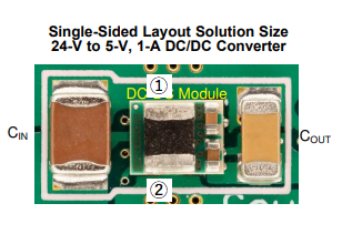
・Schematic and image (same for abnormal and normal boards)
VCC=33V

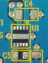
Is there a possibility of unexpected connection with adjacent  pin, GND or VCC.

---

I appreciate your great help in advance.

Best regards,

Shinichi

  • Hi Shinichi,

    Can you provide the following below:

    • Date code / Lot code of LMZM23601. This should be available on the reel package information. 
    • Is your application at elevated temperature during failure condition? Is this a time zero failure or does this failure happen after some time of operation?
    • Probe the SW at light load to see switching operation during PFM condition. This can be done by probing the top side of the exposed inductor. Please be careful when probing the switch node. If SW is unintentionally shorted to GND somehow, the device will be permanently damaged. Doing this will help me understand if part is switching as expected.

    Regards,

    Jimmy 

  • Hi Jimmy,

    Thank you for your reply.

    (1)Date code 1849 and The Lot code 0210299ZBR/0220971ZBR

    (2)The trouble phenomenon occurs immediately after the power is turned on.

    (3) I cannot understand how to confirm the waveform.

    Which is measurexd, Voltage or Current.

    The inductor current needs to use current probe.

    in this case the inductor has to remove and it is necessary to remove the inductor and modify it so that the current probe can be attached. 

    When Voltage, should the probe simply touch the inductor?

    I appreciate your great help and cooperation.

    Best regards,

    Shinichi

  • Hi Shinichi,

    I should have been more clear. Please probe the SW node so I can see the voltage and switching period. This can easily be done by touching the top side of the inductor. Again be careful not to accidently short the SW to GND as this will damage the part.

    I will run this date code and lot code by a quality engineer to check up its history.

    Regards,

    Jimmy 

  • Also how many failures do you have using this reel of devices? 

  • Hi Jimmy,

    Thank you for your reply.

    I understand it should be confirmed VSW.

    Which side should be probed with 1pin mark side(1) or the other(2).

    The failure rate is 6 failures of 22 total.

    I appreciate your great help.

    Best regards,

    Shinichi

  • Hi Shinichi,

    Please probe side "1" for the SW node of the inductor.

    Also can you provide me with your email address. I'd like to pull this offline and get you in contact with our customer quality engineer to further discuss this issue. 

    Regards,

    Jimmy 

  • Hi Jimmy,

    Thank you for your reply.

    I understand (1) side should be probed.

    I'll share this information witi the customer.

    My e-mail address is inoue-s@macnica.co.jp

    I appreciate your great help and cooperation.

    Best regards,

    Shinichi

  • Hi Shinichi,

    Thank you for providing your email address. I've contact you offline and included our quality engineer who can help provide more information on this part.

    In order to consolidate this troubleshooting process, I will be closing this thread.

    When your customer gets a chance to provide the switching waveform of the part at PFM mode no/light load, please attach it to your offline reply. 

    Thank you for using the E2E forum.

    Regards,

    Jimmy  

  • Hi Jimmy,

    Thank you for your reply.

    All right.

    I'll contact you by email.

    I appreciate your great help and cooperation.

    Best regards,

    Shinichi

  • Sounds good. Thanks for the reply.

    Regards,

    Jimmy