This thread has been locked.

If you have a related question, please click the "Ask a related question" button in the top right corner. The newly created question will be automatically linked to this question.

TPS73601 Reference value errors?

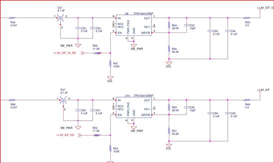
I have several TPS73601DRBT parts in an application that (should) output 1.8V and were considerably lower.  It seems the references are varying from 1.106 to 1.110 V.  When I changed the divider values to correct for this very low reference voltage the output voltage is as expected. Input voltage is 2.2725 V (measured.)  The feedback divider current is right at 40 microamps. 

I've stuffed a half dozen parts and this really has me worried as I'm risking high cost parts downstream if this doesn't work correctly. 

  • Thank you for choosing Texas Instruments LDOs.  I'm confident we'll be able to find a solution to your problem.  I"m going to need to ask some additional questions.  Can you post your LDO schematic?  What is the load current?  Is the problem still present if you increase the input voltage?  Are you measuring the input voltage right at the input to the TPS73601 or at a connector?  Are you measuring the FB voltage from the FB pin to the GND pin.  I ask because some problems are resolved by adjusting the measurement locations to eliminate I*R drops in the PWB.  Layout is also critical to ensure that IR drops don't cause a problem.  It is important that the resistor dividers do not connect to any high current traces.

  • Thank you for choosing Texas Instruments LDOs.  I'm confident we'll be able to find a solution to your problem.  I"m going to need to ask some additional questions.  Can you post your LDO schematic? 

    I'll be able to as soon as I cut and paste the image, but it's essentially the datasheet schematic and parts list..

    What is the load current? 

    The case I'm discussing here is unloaded (<1 ma,) though we have operating loads through 200 ma.

    Is the problem still present if you increase the input voltage? 

    This is difficult to do, but I'm queuing a board to mod to do exactly this.  The input voltage is over 2.27 volts, are you saying that an unloaded regulator might not regulate with 400 mv of headroom under some conditions?

    Are you measuring the input voltage right at the input to the TPS73601 or at a connector?

    Across the input (and output, for the output voltage) bypass caps which have very short runs (few mm worst case.)

      Are you measuring the FB voltage from the FB pin to the GND pin. 

    FB voltage is being measured across the FB resistor, though a check of FB pin to ground is the same to within the limits of our 5-1/2 digit VM.

    I ask because some problems are resolved by adjusting the measurement locations to eliminate I*R drops in the PWB. 

    Been there, done that, have the T shirt.   I do quite a bit of high current switcher work, so I'm very sensitive to this issue. 

    Layout is also critical to ensure that IR drops don't cause a problem. 

    Yup, done a lot of these and a lot of switchers. The layout is very compact and pretty much everything references the part ground paddle.

    It is important that the resistor dividers do not connect to any high current traces.

    We've been careful to avoid this (but we're not perfect!)

    Something else I should mention is that these all passed initial post fab tests.  While all I have is Go/NoGo data, these supplies all seemed to have met spec when first built a few weeks ago.  

  • I should also mention that only one of the two input and output bypasses are stuffed.  I left some slots for troubleshooting and optimization.

  • The layouts aren't optimal, but I don't see anything that sticks out that would specifically cause this problem.  What is your input voltage and what does the startup waveform look like?  Although the TPS73601 datasheet doesn't require large amounts of input capacitance, more is always better.  It's also important to connect the capacitors directly across the Vin and GND pins to minimize board inductance   Can you provide scope pictures of the Vin, Vout, and Vfb voltages at startup.  We've seen design with small input capacitors that have ringing on the input voltage at turn-on.  If the ringing goes above the abs max of 6V, it could damage the IC.

  • We may have just found the problem.  At least we found a major problem.  The feedback loop and power ground were referenced to two different power planes that were ~200 mV apart.  Not intended, but it crept in.


    What is "not optimal" about the layouts? (You, know, beyond the fact we messed up the grounds. )

  • Recommendations for the layout would be to connect input capacitors with short wide traces between Vin and GND.  I would also connect them without vias.  You can connect the ground side of the capacitors to the thermal pad which is connected to GND.  I'm glad to hear that you were able to find the problem.  I'll close out this thread.  Please let us know if you have additonal questions by opening another thread.