Other Parts Discussed in Thread: UCC23513
Hi all,
I looked at section 6.2: Output Split Supply, and I have some questions:
1. What is the difference between single and double supply? What is the purpose of a single supply if we are talking about Split Supply operation?
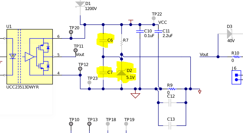
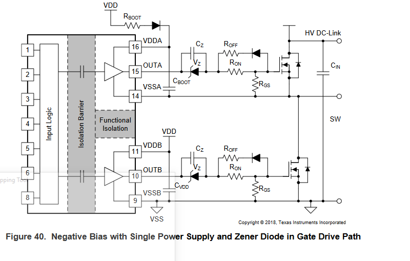
2. In the first method (Single supply), what's the purpose of the zener diode and resistor branch? From the diode's specification, it seems it's protecting against VSS voltages lower than -5V, so why is the resistor in series with VCC?
Regards,
shay