This thread has been locked.

If you have a related question, please click the "Ask a related question" button in the top right corner. The newly created question will be automatically linked to this question.

UCC28742: Flyback DC-DC converter doesn't work with the selected controller

Part Number: UCC28742
Other Parts Discussed in Thread: TL431

Hello everyone,

I'm trying to design a flyback converter with the following characteristics:

Vin: 48V (nominal voltage) ; the input voltage may vary from 40V to 56V, so I've considered  40V as minumum Vin, in the project calculations.

Vout: 230V

Pout max: 80W

Efficiency:85%

Fs:74,494kHz

It works in DCM mode. 

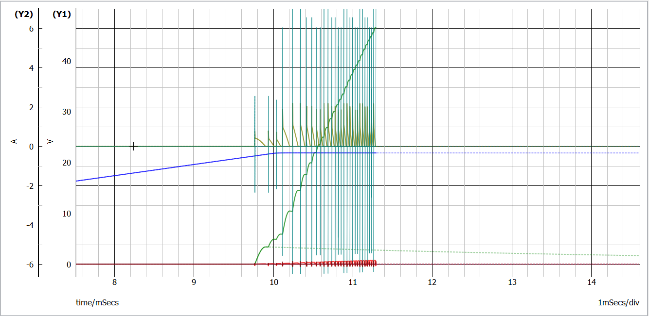
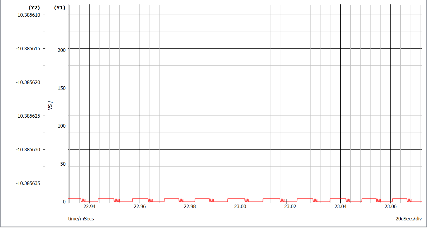
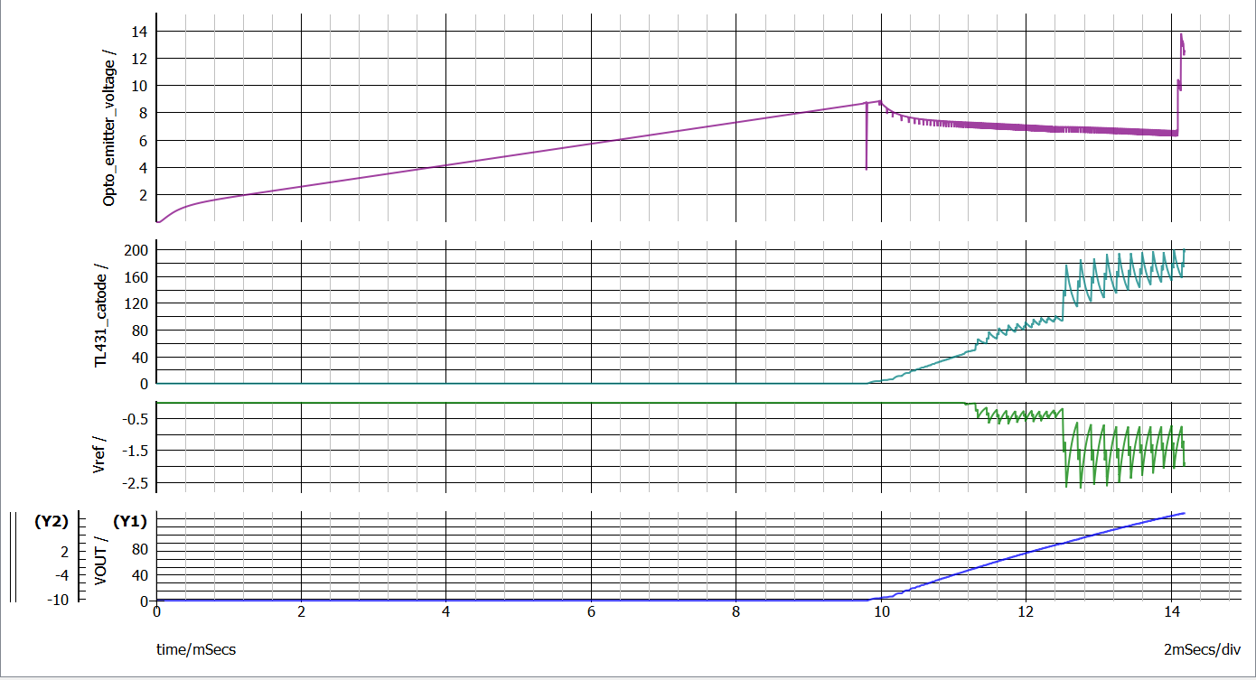
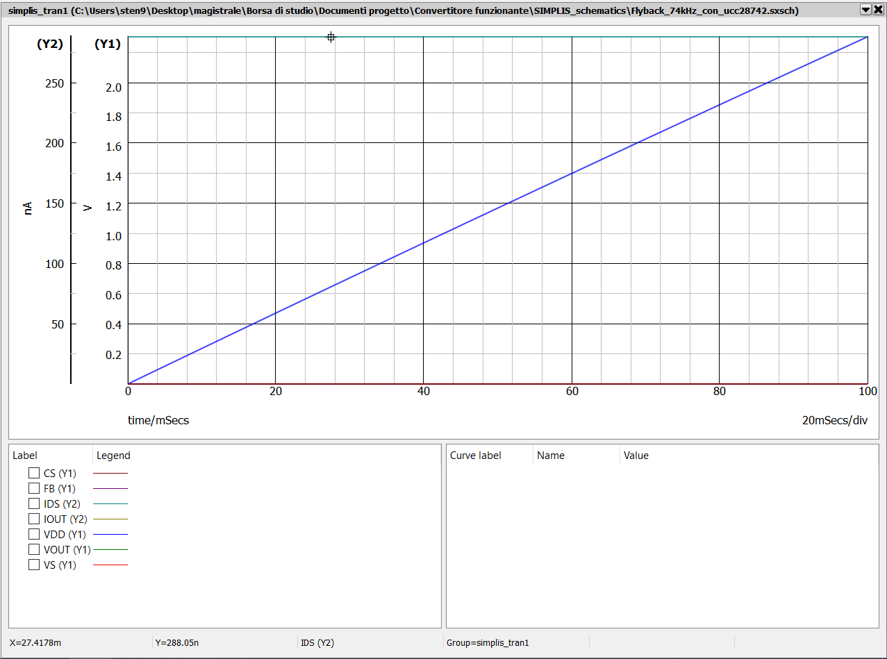
I tested the power train of the circuit with the SIMPLIS simulator, applying a 74kHz generator on the gate of the MOSFET and in this way it works, in fact the output voltage converges to 230V, but when I go to insert the controller model in the circuit it no longer works and I get the results shown in the attachment.

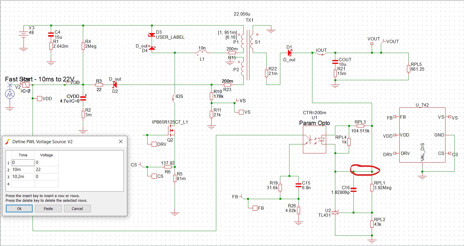
The controller was inserted in the circuit by copying, from the model available on the website(UCC28742_10W_TRANS.sxsch), the symbol and the encrypted spice code, in my simulation file.

I also tried to modify the file "UCC28742_10W_TRANS.sxsch" with my parameters, but the result is the same.

I want to say that the circuit wich I've sent is the once produced by WEBENCH.

 Where am I wrong?

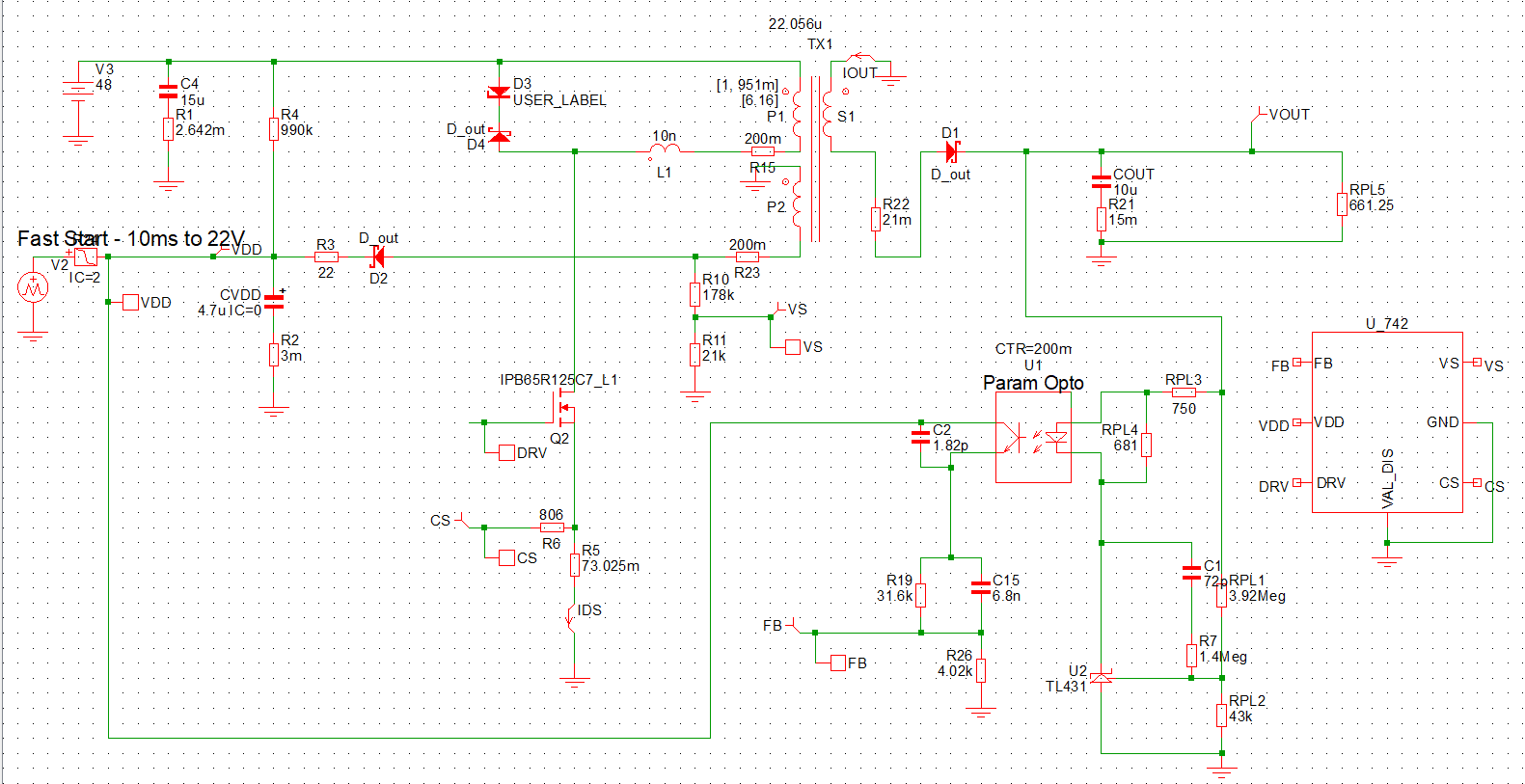
This is the circuit:

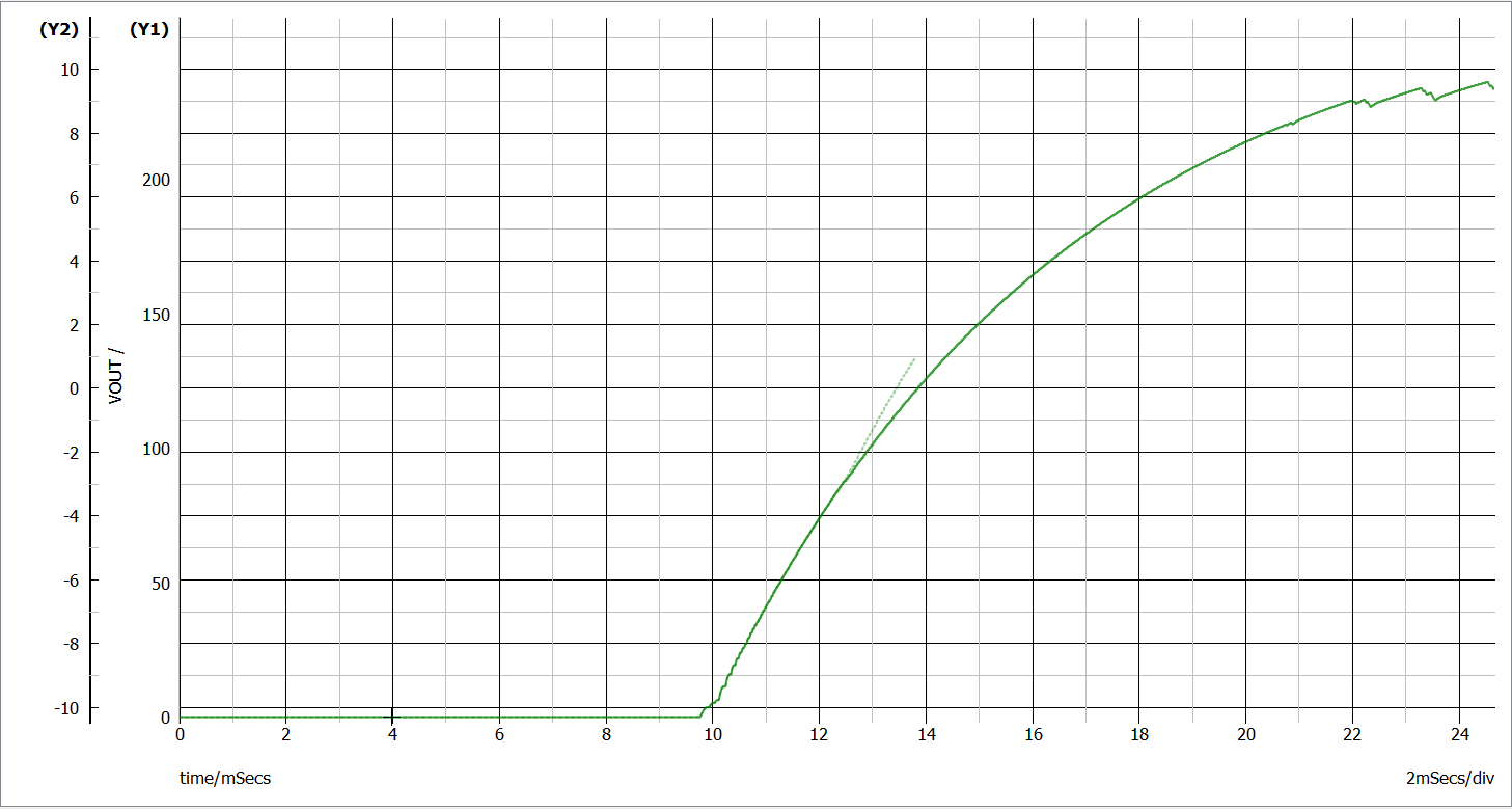
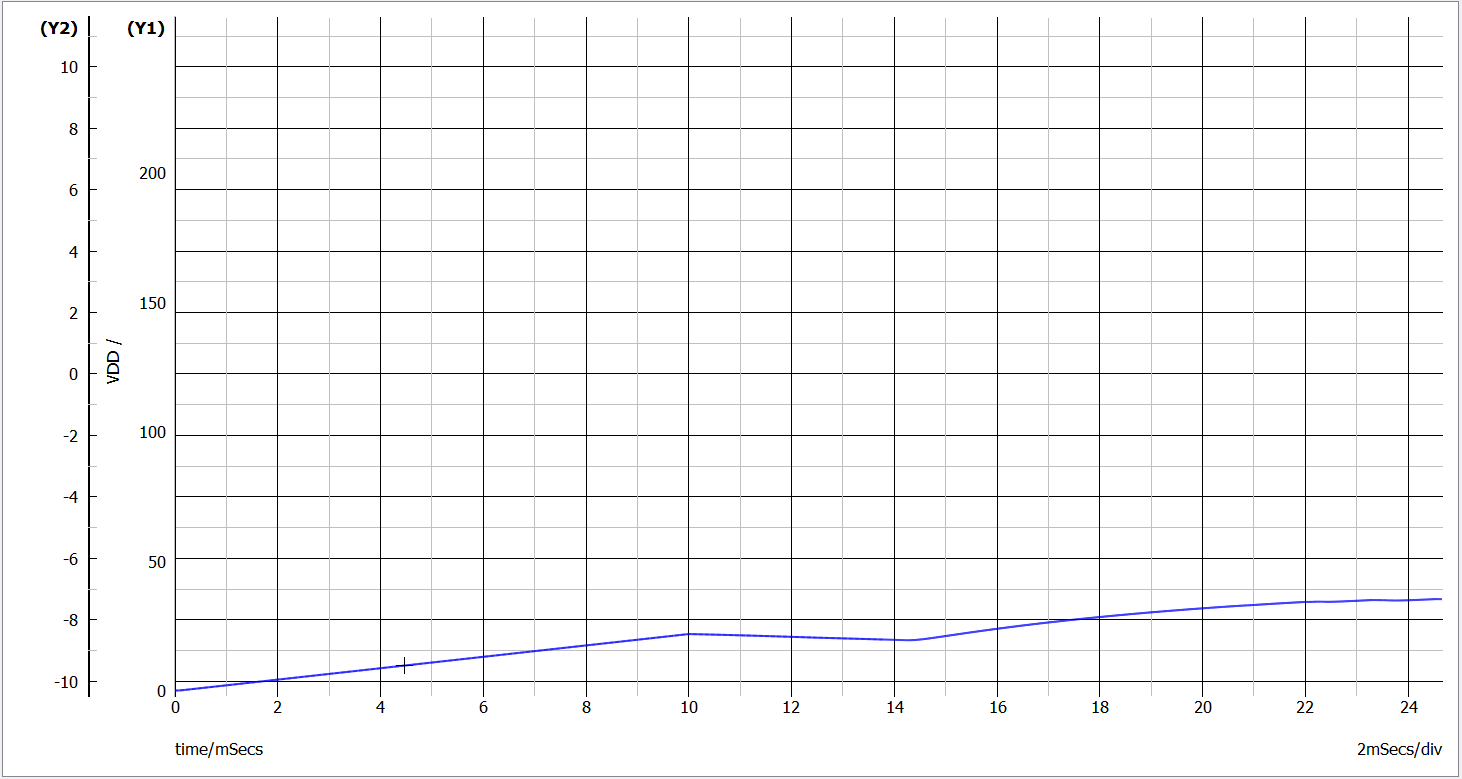
And this is the simulation result:

As you can see I tried to make changes to the circuit produced by WEBENCH, to solve the problem, but I failed.

The circuit produced by WEBENCH is attached.

Confident of your response, thank you for your attention.

WEBENCH_flyback_conv2.pdf

  • Hello Federico,

    Thank you for your interest in the UCC28742 flyback controller.

    From the 100-ms simulation result, it looks to me like the simulation is working, but needs a lot more time to start up.

    The result graph shows VDD has risen tp ~2V in 100 ms. The IC will not start switching until VDD has reached 21.6V, which will take about 1.1 secs to reach.
    This may require considerable CPU simulation time, so we often add a DC pulse source to the model to pre-charge the VDD cap to nearly 21.6V to reduce the charge-up time.   This source is diode-coupled to VDD, and provides a pulse of 20~21V for about 1ms, then goes to zero and stays off.

    Please try that idea in your simulation to eliminate a lot of charge up time.

    Regards,
    Ulrich

  • Hello Ulrich,

    Thank you very much for your advice, in fact by applying them the circuit starts and the controller pilots the MOSFET making it switch. Unfortunately, I believe there are other errors, becouse after about 11ms the simulation stops and gives me a series of errors.

    This is the circuit after the changes:

    And the simulation result is the following:

    when the simulation freezes, I can show into the command line the following errors:

    What could generate these errors?

    Thanks for the attention.
    Confident of your answer,
    Regards,
    Federico.

  • Hello Federico,

    Well, the fast start circuit works as expected, and you are getting start-up switching up to 11.3ms.

    From what I can interpret from the listed results, it looks like the simulation math expects to see -2.9 MV at Cout and Iout probe.
    I think the position of the current probe is causing a convergence error.

    I suggest to move your IOUT probe to be ahead of D1 anode, or better yet - in series with the GND pin of the secondary winding S1.  I think it will be "happier" there and the current waveform will be the same.

    Regards,

    Ulrich

  • Hello Ulrich,

    With the new changes applied, the simulation continues. I followed your suggestions, and in addition I had to make a circuit modification, because there was an error, which I show you below to get you a complete picture of the situation.

    The error is the one circled in red, plus I inserted a type 2 compensating network, because even if the simulation is blocked at the point shown below, at the point where the simulation is blocked it was already reaching 250V.

    At this point, thanks to your advices, we are moving towards the correct functioning of the circuit. Since for all the attempts made over the weekend I always get the same error, I can't understand if it is a circuit problem or is a simulation setting problem.

    For this reason I want to show you the waveforms individually.

    This is the circuit with the ugraded circuit discussed previously:

    As you can see I have changet the compensation Network and I've moved current probes as you suggested.

    Following I show you all foundamentals waveforms:

    VOUT:

    FB:

    CS:

    VS:

    IOUT:

    IDS:

    And finnaly the error that occurs during simulation:

    I hope that with further advices from you I can take a few more steps forward. Also to get a complete picture of the circuit I also send you the zip file, with the simulation file.Flyback_74kHz_con_ucc28742.zip

    Thanks for the attention.
    Confident of your answer,

    Regards,

    Federico.

  • Hello Federico,


    Unfortunately, I am not in a position to run your Simplis file. However, I do have some observations about your new schematic diagram that you can check:


    1. A real TL431 has a maximum Vka range of about 30V. Your design is connected to a 230V output.   I don’t know how the TL431 model behaves when over-voltaged this way, but I suggest to connect RPL3 to a 12-V source instead of to VOUT.

    2. C1 is too small (72pF) and R7 is too big (1.4M). This is basically open-loop.   I suggest to have C1 = 0.1uF and R7 = 100ohm. This will have slow transient response, but should be stable, and you can optimize response later after getting the main circuit running properly.

    3. I am concerned about the IDS graph showing +10A and -10A peaks.   You may see some negative current (< -1A) in the source leg due to turn-off gate-drive, but -10A does not seem correct.
      I suggest to expand these pulses to see if the negative currents are just spikes (from Coss) or if they contain significant energy. Or maybe it is L-C ringing of lead inductance with gate capacitance. I suggest that you add a 10-ohm resistor in series between DRV and the Q2 gate.

      Lastly, I suggest that you rename the IOUT current probe to ISEC, since that is what it is measuring. I would consider IOUT to be the load current after COUT.

      Regards,
      Ulrich

  • Hello Ulrich,

    I am writing to you because I made the changes you suggested, but I always have the same problem. But you were right about the TL431, and I think the problem is there and that it concerns the voltage ratings I need.

    So at this point I show you the simulations that I get with the old configuration and those that I get with the new one, suggested by you.

    Whit the old circuit configuration:

    I put voltage probes on the OPTOcoupler output emitter, on the cathode of the TL431, and on the input of the Vref pin. And the simulation result is the following:
    With the compensation network shown in the figure the result is:
    with the compensation network suggested by you, the result is:
    Now, applying 12V on RPL3, the circuit is the following:
    And the simulation result is:

    as you can see in all the attempts made the same thing always happens.

    The error given by the simulator, in the last example I've shown you, is the following:

    I also tried to derive the 12V from the converter output through a voltage divider, and then from the 12V obtained, with a further divider I obtained the VREF, but the results of this solution were much more bad than those shown, so I rejected it as a solution. Moreover I also tried to add another output to the transformer, to get the 12V, but also in this case I got bad results. 

    So I start thinking about having to change TL431, or not to use it and looking for other solutions .... 

    What do you think about this results?

    If you have other solutions, even if they change the circuit topology, I can evaluate them.

    Furthermore, I can't reduce the peaks of the IDS with the 10 ohm resistor, so I think it is a resonance problem between the output capacity of the MOSFET and the leakage inductance.

    In the end I thank you for the various advices , and I hope that in the end we will make the circuit work.

    Confident in your answer,
    Regards,
    Federico.

  • Hello Federico,

    I'm surprised at the TL431 voltage... I don't know how it can get to 300V with a 12-V source pull-up.

    The other voltages also don't make sense. 

    Until the simulation reaches the error point and stops, it is running although with strange trends.

    I suggest to break up the schematic into an open-loop pwm driver to the MOSFET and into a TL431 circuit, separately.

    Break them into small manageable chunks and make sure each sub section simulates as expected. Debug the ones that don't. Then assemble sub-chunks into larger circuits and makes sure those behave as expected.  They don't have to be closed loops, but the outputs of each subcircuit should change in an expected manner based on the inputs.  

    Once all of them work, assemble back into the UCC28742 flyback and hopefully it too will work.

    Regards,

    Ulrich