This thread has been locked.

If you have a related question, please click the "Ask a related question" button in the top right corner. The newly created question will be automatically linked to this question.

UCC21750-Q1: How to connect CLMPI pin when BJT-CB is used? how to implemement AMC function with potential long AMC loop?

Part Number: UCC21750-Q1
Other Parts Discussed in Thread: UCC21750, UCC21732

Hi expert,

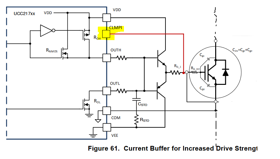
I would like ask two questions about the active miller clamping (AMC) function of ucc21750. According to D/S, ucc21750 provides the internal miller clamping pin (CLMPI).

Questions are as follows.

1. If extra BJT-CB (>10A) is required for SiC mosfets, where to connect CMLPI pin? I found there maybe a website link about this question in E2E, but it is not available anymore. Could you please explain this question again? I think that CLMPI should be directly connected to gate terminal of power mosfets with 0Ohms resistor, but I am not sure.

2. If the CLMPI pin has to be far away from its connection target, could you please give some suggestions to keep AMC function effective. For example, if the extra BJT-CB is introduced, AMC loop becomes longer with increased impedance, which would negatively affect AMC performance. I found some people connect CLMPI pin with an external PNP transistor (is placed next to gate terminal) to form AMC function. How do you think about this kind of method and do you have any suggestions to implement this method? Or do you have any other better solutions?

Since we are using ucc21750 to drive expensive mosfets. Any valuable information you provided will help us reduce the risk. Appreciate your response and help. 

Bests,

Zack

  • Hi Zack,

    These are good questions!

    Zhehui Guo said:
    1. If extra BJT-CB (>10A) is required for SiC mosfets, where to connect CMLPI pin? I found there maybe a website link about this question in E2E, but it is not available anymore. Could you please explain this question again? I think that CLMPI should be directly connected to gate terminal of power mosfets with 0Ohms resistor, but I am not sure.

    CLMPI can be connected directly to IGBT gate even when used with a current buffer, as shown in the figure below.

    If you want a higher current than the Built-in Miller clamp current of 4A, you can use the circuit below, with a PNP to pull down the gate.

    I am not sure if you have determined you need a higher current than this.

    Note that CLMPI should be connected to gate by a thick trace to reduce parasitic inductance and the distance to the gate should be minimized as much as possible.

    When it says CLMPI, as we know its "Internal miller clamp", meaning there is an internal MOSFET as well as comparator tied to the pin that both senses and pulls down the gate voltage thru the same pin.

    When we use the CLMPI pin with PNP pull down circuit in the second figure, the sense function HAS to be tied to the gate somehow, so the Resistor from Emitter to Base, its purpose is to tie this without shorting out the PNP to sense when the Miller clamp threshold has been reached. Once its reached, the internal FET will pull down, allowing the base current to flow and the PNP will be a "stronger" miller clamp pulldown than the internally, but we can see that the internal one also can pull the gate with some current which depends on the resistor values. If you need more explanation on this, let me know. There are some considerations to use this circuit.

    Zhehui Guo said:
    2. If the CLMPI pin has to be far away from its connection target, could you please give some suggestions to keep AMC function effective. For example, if the extra BJT-CB is introduced, AMC loop becomes longer with increased impedance, which would negatively affect AMC performance. I found some people connect CLMPI pin with an external PNP transistor (is placed next to gate terminal) to form AMC function. How do you think about this kind of method and do you have any suggestions to implement this method? Or do you have any other better solutions?

    If the IGBT gate is located quite far there is some options that we could recommend. The option i mentioned earlier would be using the PNP pull-down attached to CLMPI, which can work.

    We also have variants within the UCC217xx specifically designed to solve this type of problem UCC21732 and UCC21736, and they actually have "External Miller clamp, which is shown by CLMPE pin.

    Essentially, the CLMPE pin just drives a N Mosfet that you can place very close to the gate, the circuit is shown below. You can tune the current with the mosfet choice as well as a resistor connected from MOSFET drain to the gate of IGBT.

    When using either this or the circuit with PNP, you have to consider some things, roughly:

    When using CLMPE, the miller clamp threshold is measured at OUTL pin,  so there will be some difference in the voltage at the gate and whats measured at the pin since a buffer is used (VBE drop, resistor drop etc), but this doesn't affect the efficacy of the miller clamp system.

    Similar concept applies to  when using the CLMPI pin with PNP pulldown, youre measuring it at the pin which is connected to gate by teh Reistor and PNP

    However, if you choose one of those, there are difference in the features set, which i've highlighted below. Specifically, one has 2LTO+STO instead of only STO, and UCC21736 has higher STO current . One does NOT have the Analog-to-PWM channel, but rather "active short circuit" which you probably may not have any use for.

    Both also have OC detection rather than DESAT. OC can be configured to be be used as DESAT, but its a difference thats worth mentioning.

    Hopefully this helps with your questions. If I've answered your questions, please let me know by pressing the green button. And dont hesistate to follow up here if you need clarification or have additional questions.

    best

    Dimitri

  • Hi Dimitri,

    Many thanks for your professional answers. I am very interested in the figure-2 you posted in the first question. Could you explain more details about considerations to use this circuit (CLMPI+pnp pull down method)? And a question for figure-2 in the first question: can we connect the collector terminal of pnp to VEE (such as -5V) rather than GND?

    Bests,

    Zack

  • Hi Zack,

    Zhehui Guo said:
    can we connect the collector terminal of pnp to VEE (such as -5V) rather than GND?

    Yes, in fact it should be connected to VEE! That is my mistake of not deleting "GND" in the symbol. Collector should be connected to VEE.

    Zhehui Guo said:
    Could you explain more details about considerations to use this circuit (CLMPI+pnp pull down method)?

    Due to resistors in the path from IGBT gate to CLMPI pin , there could be some delay from the gate voltage to monitored voltage.

    The other consideration is that the Gate voltage will not be pulled down completely to VEE like it could be when using the internal miller clamp or MOSFET with CLMPE pin. This is an unavoidable part of using the PNP **

    while it will be pulled down to VEE, if there is dv/dt that caused gate voltage to jump, the PNP will only turn on if there the IGBT gate voltage (PNP emitter) is at least ~0.7+VEE, so response would be a little different than with internal miller clamp, or with a FET controlled by the CLMPE pin. Since the internal/external FET will always have VGS/VTH when miller clamp is active, it should have a quicker response to jumps in DV/DT. I might simulate the PNP case and compare it to external FET.

    please let me know if you have any more questions!

    Best

    Dimitri

  • Dear Dimitri,

    Appreciate your patience and professional answers. Many thanks.

    Bests,

    Zack

  • Zack,

    I thought further about it and actually, one point that i mentioned before is incorrect.

    When CLMPI pin is being used with PNP to increase miller-clamp pulldown, it still will be able to pulldown to VEE all the way initially, with the internal miller clamp FET providing the final pull down at the point at which the PNP's |VBE| < 0.7, causing it turn off.

    I guess then, the consideration is that, while it will be pulled down to VEE, if there is dv/dt that caused gate voltage to jump, the PNP will only turn on if there the IGBT gate voltage (PNP emitter) is at least ~0.7+VEE, so response would be a little different than with internal miller clamp, or with a FET controlled by the CLMPE pin. Since the internal/external FET will always have VGS/VTH when miller clamp is active, it should have a quicker response to jumps in DV/DT. I might simulate the PNP case and compare it to external FET.

    I will modify my above response to avoid future confusion.

    Thank you,

    Best

    Dimitri

  • Hi, dimitri,

    I'm interesting in the pics and tables you've posted. May you provide the source of them ? Thanks.

  • diverger said:

    Hi, dimitri,

    I'm interesting in the pics and tables you've posted. May you provide the source of them ? Thanks.

    Hi,

    We don't have these shared on the web anywhere. We have some comparison tables on E2E

    Best

    Dimitri