This thread has been locked.

If you have a related question, please click the "Ask a related question" button in the top right corner. The newly created question will be automatically linked to this question.

LM61460-Q1: Vin decreases in TINA simulation with inverted Vout

Part Number: LM61460-Q1
Other Parts Discussed in Thread: LM61460

Hello,

I'm trying to make -13.5V from a 13.5V power supply using LM61460, which I'm also using it for positive supply buck conversion.
I referred to the inverting buck-boost converter design documents by TI and came up with the values below.
Blue letters are the calculated values.

LM61460
Nominal Input Voltage 13.50 V
Input Voltage ripple 1.00 %
Output Voltage -13.50 V
Outpu Voltage Ripple 0.50 %
Max Ouput Current 2.00 A
Vref 1.00 V
Rfbt 806.00 ohm
Rfbb 10075.00 ohm
Krp 0.25  
Duty Cycle 0.50  
Minimum Current Limit 8.90 A
Inductor Ripple Current 2.23 A
     
Ouput Current < 3.89 A
Rt 26100 ohm
Fsw 0.52 kHz
ILavg 7.79 A
Inductor 6.72 uH
ILpeak 8.76 A
ILrms 7.81 A

I chose the RT resistor value of 26.1k to use a 6.8uH inductor that I have.

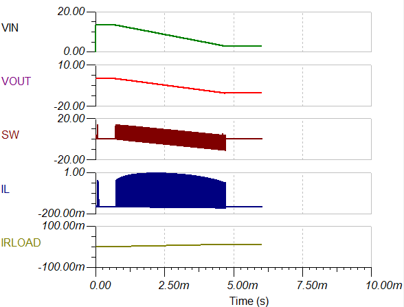
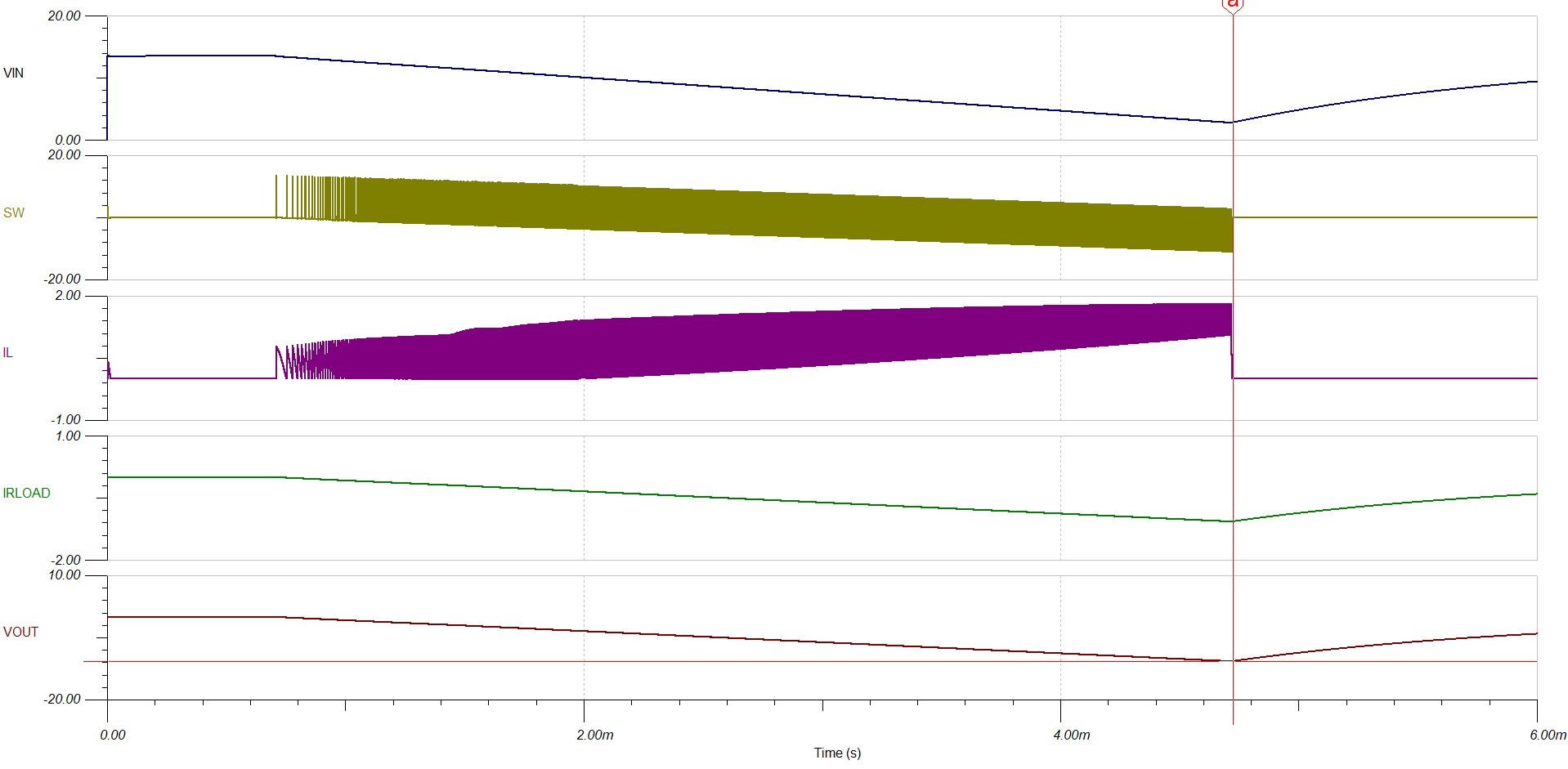
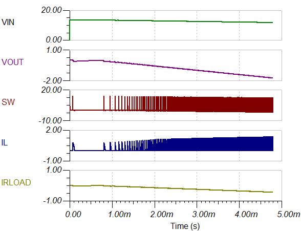
But like the attached pictures. When I simulate it in TINA, the Vout goes under 0V but doesn't reach -13.5V.
What's even more strange is that the Vin decrease as the Vout goes lower.
I tried changing input and output capacitor values, deleted start-up condition, and the load resistance.
I also tried using snvmbx3 example and snvmbx5 example, but there was no change.

Is LM61460 not suitable for inverted supply?

snvmbx3_13.5V to - 13.5V

snvmbx3_13.5V to -13.5V_Vin drop.TSC

snvmbx5_13.5V to - 13.5V

snvmbx5_13.5V to -13.5V_Vin drop.TSC

  • Hi Brian,

    I will check your circuit and update you later.

    B R

    Andy

  • Hi Brian,

    I ran the simulation with slightly different configuration in a sense that i connect the input voltage between VIN and VOUT instead of VIN and GND. 

    I attached the 2 files above. The reason why VIN looks like it's falling is because the reference is taken from GND. You need to attach a voltmeter across like what i did on the VOUT to see the actual reference point of VIN

    I noticed that on your schematic, you have another resistor in parallel with 10k and i remove that and also the RT resistor should be connected to -VOUT in the circuit

    IBB_LM61460_v1.TSCIBB_LM61460_v2.TSC

  • Hello Arief,

    Thanks for the answer.

    I checked your files and trying to understand the difference between v1 and v2.

    I noticed the voltmeter in v1 schematic, but I couldn't find a way to read(?) the voltage. Is it just the same as a regular node?

    And to my understanding of v1's Vin is referenced to Vout and v2's Vin is a reference to ground.

    In the transient simulation, v1 gives -13.5V but the v2 gives +13.5V

    id you make 2 simulation files to illustrate the Vout voltage can change by where we reference the Vin ground to?

    Sorry for the questions, it's my first time make an inverted buck-boost controller so it's taking time to understand the schematics and how to use the sim tool.

    Best regards

    Brian

  • Hi Brian,

    No worries, let me see if i can address your question. 

    v1 and v2 is meant to show the same idea. Even in v2 the VIN is referenced to VOUT. Sorry if the trace somewhat misleading. You can see that it still referenced to VOUT. The probing on the VOUT can be postive or negative depending on where you referenced it to. In v1 i purposely put a voltmeter in there to show that the VOUT measurement referenced to GND. 

    The reason i use a voltmeter instead of a "voltage pin" is because with voltmeter i can referenced it to anywhere i like based on the two leads. It's as if you have a handheld DMM and measuring it on the board. 

    The key point in here that the inductor node is tied to GND instead of VOUT in a normal buck configuration and that what makes it an inverting buck boost topology. All the IC reference point should now be -VOUT instead of GND. Therefore the IC pin that says "GND" should be connected to -VOUT in your schematic. 

    Here is an app note that may help clarify when you converting from buck to inverting buck boost topology

    https://www.ti.com/lit/an/snva722b/snva722b.pdf

    Thanks

    -Arief


  • Hi Arief,

    Thank you so much for the explanation.

    I changed both v1 and v2 schematics to look similar and now I can see what you are pointing.

    I will also check the document you linked.

    Best regards,

    Brian