7178.padsize.pdfI'm considering TPS7A7002 PCB board layout.
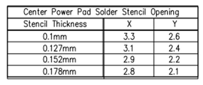
With use stencil thickness of 0.1mm,Power pad solder Stencil Opening is recommended 3.3mm(X)×2.6mm(Y)
On the other hand,Power pad geometry is 3.1mm(X)×2.4mm(Y) On Datasheet
When Use stencil thickness of 0.1mm,Power pad geometry is 3.1mm(X)×2.4mm(Y) is correct? but also 3.1mm(X)×2.4mm(Y)?