This thread has been locked.

If you have a related question, please click the "Ask a related question" button in the top right corner. The newly created question will be automatically linked to this question.

UCC28610: ZCD and LC question

Part Number: UCC28610

Hi Guys

The flyback uses UCC28610 and the output voltage is 12V. In the test, under the condition of 170V to 400VDC input, the number of ZCDs is 2 at full load.

problem:

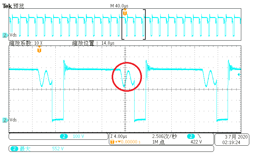
1. Why is the 170V to 400VDC input, full load (continue to increase the load, the chip is in the restart state), the number of ZCD is 2, why does not appear ZCD=1? Datasheet show: at least 1. So what will affect the number of ZCD? The following waveform (Picture 1) is 400VDC input voltage Load=4A, Mosfet's VDS. In the measured waveform, is the time for the free-wheeling (inside the red circle) 2.4 us? Is it related to the Twait (ZCD) time in the datasheet?

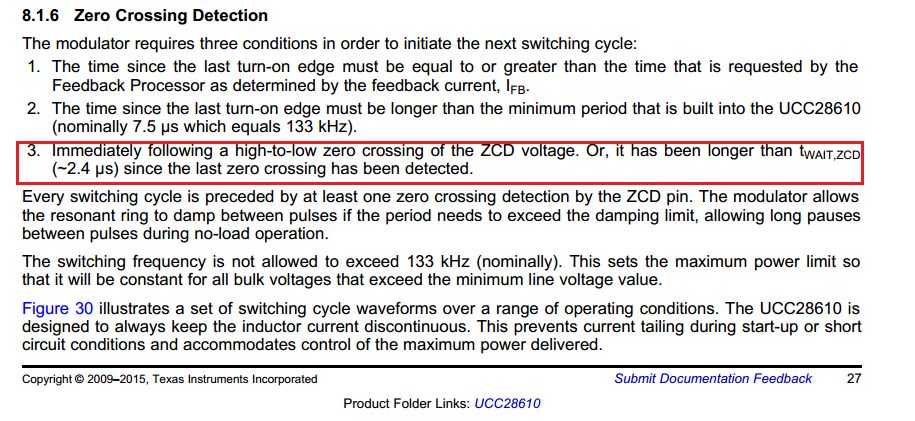
Datasheet, Page 7

Picture 1 Vin=400VDS, Load=4A, Signal 2 VDS

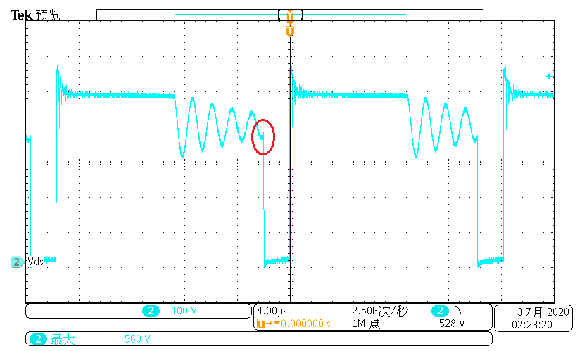
2. Observe the waveform of the VDS above (Picture 1, Load=4A). The MOSFET does not turn on Mosfet at the bottom of the resonance. The load is relatively small (Load=3A), when ZCD is equal to 5 (Picture 2), the MOSFET is close to the bottom when it is turned on.

In the case of a relatively large load (Picture 1, Load=4A), the MOSFET has not turned on Mosfet at the bottom. Is it the cause of UCC28610? I tested the waveform at 170VDC and full load at 250VDC, the MOSFET also did not turn on Mosfet at the bottom of the resonance.

Is it necessary to add the capacitor described in the Datasheet to adjust the LC resonance phase to the same phase as the ZCD current? What does the specific opening time here have to do with?

Picture 2 Vin=400VDS, Load=3A, Signal 2 VDS

3. Page27 in the datasheet. What is the meaning of tWAIT in the circle?

Does this mean that the IDRV output, or the time between Ton and the first detected ZCD, must be at least 7.5us in time difference?

Thanks

-Vincent

  • Hello,

    I reviewed the data sheet and this is a DCM fly back converter that will operate as a quasi resonant converter at full load.  It will uses AM and FM modulation to maintain the duty cycle.  It will only valley switch on the first resonant ring at minimum input voltage maximum load.   

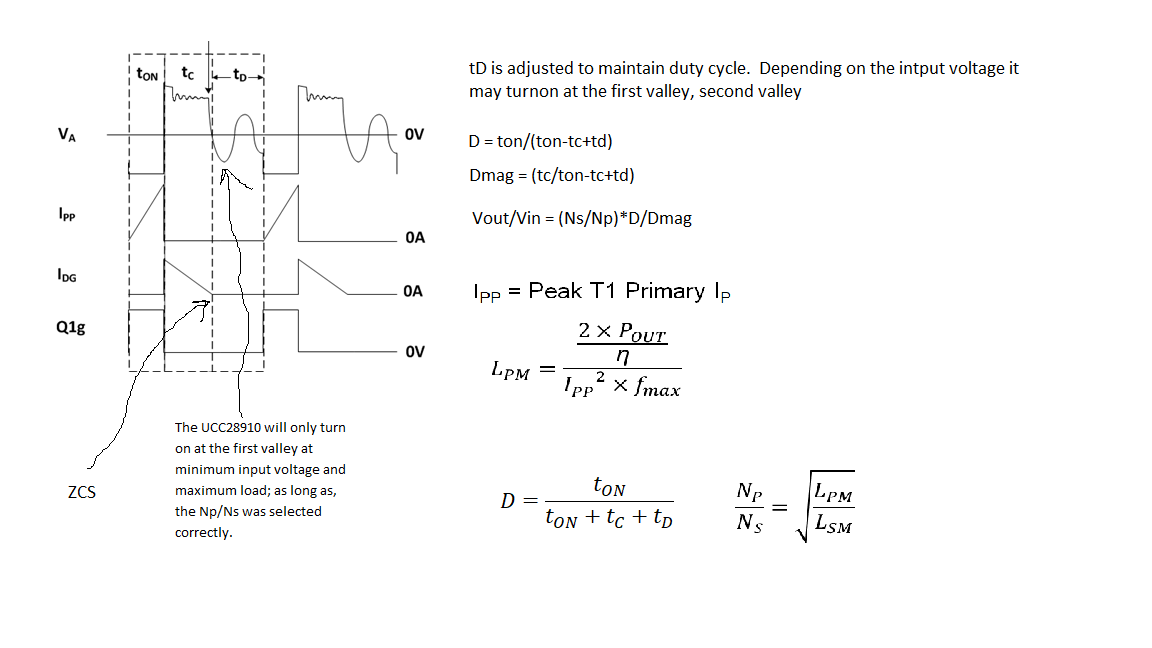
    The UCC28610 controls the peak current and monitors the aux winding.  When the aux winding has passed through ground it has determined there is zero current on the secondary.  The controller than adjusts tD to maintain the duty cycle.  I drew this diagram to show how the device operates.

    To get the aux winding switch node to turn on the FET at the first valley will only happen at the minimum input voltage maximum load, if Np/Ns was selected correctly.

    Regards,

  • Hi Mike

    thanks for your response. 

    following the control, I think the Ton point should be at the valley of the VDS damping resonant. But you can see my waveform, at 3A load, it does turn on at the valley, but 4A load doesn't. Why not turn on at the VDS valley at 4A load? 

    Does the ZCD capacitor will affect it? We adjust the Czcd at the ZCD pin. When we choose very low capacitor ~5pF. This system will not operate normally. And we can't see the ZCD waveform either. We adjust this cap to ~nF, it will be OK. Why?

    Thanks

    -Vincent

  • Hello Vincent,

    The UCC28610 after it has detected a ZCD pin crossing zero it will wait 400 ns and then turns on the gate drive.  This is not true valley detection.

    The waveform that you are observing is similar to figure 12 of the UCC28610EVM-474 user's guide which you can find at the following link.

    If your resonant tank frequency is faster than 1/(4*400ns) = 625 kHz the FET will not turn on at the valley but on the up swing as you are observing and was shown in the EVM users guide for the UCC28610. 

    The ZCD pin also detects output over voltage while delivering energy to the secondary.  This is sensed after TBLANK of 1 us during tc of the diagram I sent previously.  If the ZCD pin sees more than 5 V OVP will be triggered and switching will be stopped and VDD will cycle between VDDoff and VDDon in fault mode until the fault is removed.  This is explained in section 7.3.4 in the data sheet.

    If you have excessive ringing on the ZCD pin this could trigger and OVP fault.  You mentioning that you needed nF of capacitance on the ZCD pin to get the controller to work.  This would indicate that there is excessive aux winging ringing and most likely the controller is shutting down to an OVP fault, which filtering has removed.

    I wonder if the capacitance you are adding is causing too much delay to the ZCD pin causing more hard switching then needed. I would think that you would not need more than 100 to 220 pF on this pin.  Could try reducing that capacitor see if things improve.

    Regards,