This thread has been locked.

If you have a related question, please click the "Ask a related question" button in the top right corner. The newly created question will be automatically linked to this question.

BQ76PL455A-Q1: Unable to setup UART Communication between MCU and BQ IC

Part Number: BQ76PL455A-Q1

Hello,

I have been trying to connect the BQ76PL455A-Q1 (BQ ic for short) to my MCU on a custom board. I am only using a single BQ ic chip right now and have no plans to do any daisy-chaining to this chip. I have added the required pull-ups resistors and other resistors and capacitors as mentioned in the design reference document. 

Here are the voltages I observed in Idle state:

  • V5VAO = 5.1V
  • VP/VDIG = 5.3V
  • VIO = 3.3V
  • RX = 3.3V in idle state
  • TX = 3.3V in idle state

After checking voltages, I was looking to set up communication and I sent out the following commands: 

#define buf1_len  (4 + 2)
#define buf2_len  (3 + 2)
#define buf3_len  (3 + 2)
#define buf4_len  (3 + 2)
#define buf5_len  (5 + 2)
#define buf6_len  (4 + 2)
#define buf7_len  (4 + 2)
#define buf8_len  (4 + 2)
#define buf9_len  (4 + 2)
#define buf10_len  (5 + 2)
#define buf11_len  (4 + 2)

char buf1[buf1_len] = {0xF2, 0x10, 0x10, 0x80, 0x3F, 0x1D};
char buf2[buf2_len] = {0xF1, 0x0E, 0x10, 0x54, 0x5F};
char buf3[buf3_len] = {0xF1, 0x0C, 0x08, 0x55, 0x35};
char buf4[buf4_len] = {0xF1, 0x0A, 0x00, 0x57, 0x53};
char buf5[buf5_len] = {0x92, 0x00, 0x52, 0xFF, 0xC0, 0x59, 0xAC};
char buf6[buf6_len] = {0x91, 0x00, 0x3D, 0x00, 0x3C, 0x6C};
char buf7[buf7_len] = {0x91, 0x00, 0x3E, 0xBC, 0x3D, 0x2D};
char buf8[buf8_len] = {0x91, 0x00, 0x07, 0x00, 0xCC, 0x2E};
char buf9[buf9_len] = {0x91, 0x00, 0x51, 0x38, 0x10, 0xBE};
char buf10[buf10_len] = {0x92, 0x00, 0x52, 0xFF, 0xC0, 0x59, 0xAC};
char buf11[buf11_len] = {0x81, 0x00, 0x51, 0x00, 0x15, 0xAC};

delay_ms(100);

sci_user_write(buf1, buf1_len);				delay_ms(10);
sci_user_write(buf2, buf2_len);				delay_ms(10);
sci_user_write(buf3, buf3_len);				delay_ms(10);
sci_user_write(buf4, buf4_len);				delay_ms(10);
sci_user_write(buf5, buf5_len);				delay_ms(10);
sci_user_write(buf6, buf6_len);				delay_ms(10);
sci_user_write(buf7, buf7_len);				delay_ms(10);
sci_user_write(buf8, buf8_len);				delay_ms(10);
sci_user_write(buf9, buf9_len);				delay_ms(10);
sci_user_write(buf10, buf10_len);			delay_ms(10);
sci_user_write(buf11, buf11_len);			delay_ms(10);

For now, I simply hardcoded the CRC after calculating it on an online calculator. The commands above are modified from the software design reference document available for BQ76PL455A-Q1. 

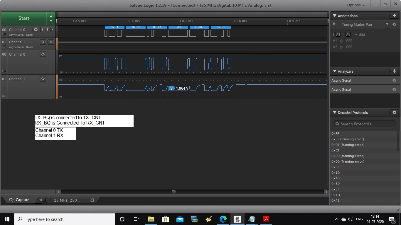
While sending out the commands, I connected a logic analyzer on the RX and TX pins of the BQ ic. In my design, I was not sure whether it is a direct connection (TX to TX, RX to RX) or cross-connection (TX to RX, RX to TX), so I have added some jumpers which will allow me to switch between both the configurations. I have added some screenshots from the logic analyzer. I am observing some data ripples on the RX line while transmitting from MCU. Also, there is no response from the BQ ic after I send out the 11th command from the above snippet of code. 

  • Hi Nishant,

    Are you able to test your custom board with either our GUI or example code first to check if there are any hardware issues? And to clarify, MCU TX->device RX and MCU RX->device TX.

    Regards,

    Taylor

  • Hello, 

    I have not been able to connect to the GUI using a CP210x chip I had lying around. However, from this POST I understand I would need to connect to the GUI via an FTDI chip. I tried to do so by connecting the FTDI chip of an Arduino Uno, but I was not very successful with that (most likely a voltage mismatch in UART comm). I will update more once I have access to an FTDI chip working at 3.3V. [limited resources, Covid-19 :( :(]

    The MCU on my board is not from TI, so I am translating the example code into my MCU's syntax. Working on that still. The commands I mentioned in the original post however are from the software design reference document. Close to what the example code dictates. 

    The Wakeup Pin: I initially pull it down to logic '0' and then snap it back up to '1' to wakeup the system and let it stay at '1' till I am ready to shut down the system again. I start my communication with the Battery Monitor IC say 100ms after the wakeup is pulled to '1'. Is this sequence okay? 

  • Hi Nishant,

    It is possible to order the FTDI cable separately if you did not get an EVM with it included. It is TTL-232R-5V. I understand the limitations, no worries. And no, it is actually not good practice to allow the wakeup pin to float to 1 as it may cause unintentional wakeups. You want to 0-1-0 transition and keep it low until wanting to wakeup again.

    Regards,

    Taylor

  • Hello,

    I am working on getting the results of connecting the GUI to the Battery Monitor IC. I am not using an EVM, rather I am attempting to directly connect the UART of the USB to TTL converter to the UART of the BQ76PL455ATPFCTQ1 IC.

    I have added 100k pull-ups from RX and TX to VIO, added the 50ohm resistor in series with the UART. The Wakeup I am independently triggering from another source (all GNDs are common). 

    In the images attached to the original post, what could be the cause of the Transmitted data being reflected onto the RX line?

  • Hi Nishant,

    Can you please confirm that your connections are as follows:

    • MCU RX to BQ TX
    • MCU TX to BQ RX

    Also, please make sure you are following the recommendations listed on section 8.1.2.1 "Single-Ended Communication (UART)" of the BQ76PL455A-Q1 datasheet? You mentioned you do have a pull up on TX and RX but there is also a recommendation on how to connect the COML+/- pins. 

    Regarding your comment: "...added the 50ohm resistor in series with the UART"  Where was this resistor added? Between which pins?

    Regards,

    Leslie

  • Hello,

    The Connections are MCU RX to BQ TX and vice versa. Using section 8.1.2.1, we are following the recommendations of pull up resistors. COML+/- pins are connected to V5VA0 and GND respectively through the 100k resistors. 

    As for the 50 Ohm resistors, they are connected between

    • RX of MCU and TX of BQ
    • TX of MCU and RX of BQ

    Sincerely,

    Nishant

  • Hello,

    I managed to connect the GUI to the BQ76PL455A-Q1 via an Arduino (configured to use as an FTDI peripheral). However, for the same, I had to reconfigure the BQ ic to operate completely at 5V. I routed the Wakeup to a 5V switch, VIO to VP/VDIG via a 1Ohm resistor (mentioned in the Design Reference Document Figure 1).

    My initial config was done at 3.3V by connecting the Wakeup to a digital pin on MCU (operating at 3.3V), and VIO connected to the same supply as the MCU (an external supply of 3.3V). This connection of VIO to MCU supply is recommended in Datasheet, Section 5, Pin functions table under VIO pin description:

    "Typically, connect this pin to VP/VDIG for all devices except the base device in the stack. In the base (or single) device, this pin is typically driven from the same supply as the microcontroller I/O pins."

    The 3.3V supply is working correctly as the MCU was operating along with a couple of other peripherals connected to the same supply. I even disconnected these peripherals in case they were overloading the 3.3V line but yet the BQ IC did not operate at 3.3V. 

    While for verification purposes, the 5V config is okay, but I cannot operate my MCU and other peripherals at 5V. Is there something I might have missed while designing in the 3.3V range?  Currently, the observed Voltages levels to date are:

    • V5VAO = 5.1V
    • VP/VDIG = 5.3V

    When VIO is connected to VP/VDIG,

    • Voltage at VIO = 5.2V
    • RX and TX = 5V (in idle)

    When VIO is connected to an external supply,

    • Voltage at VIO = 3.3V
    • RX and TX = 3.3V (in idle)
  • Hi Nishant,

    Thanks for providing the additional information that Leslie requested. Let us look over your questions and get back to you tomorrow.

    Thank you,

  • Hello,

    A response would be welcome on the posted issue. 

    Thanks. 

    Nishant

  • Hi Nishant,

    It is hard to say why 3.3V would not work based on your comments vs 5V unless something is not configured correctly, but ensure you follow base device VIO connection to host side driver for logic reference rather than VP as for stack device. I see a few next step options:

    1) Scope probe 3.3V logic for RX/TX/VIO/GND to see if its really high enough to meet Vio thresholds of device.

    2) Install level shifter or digital isolator between host mcu and BQ to shift 3.3V logic to 5V. This is how we drive our next gen devices with 3.3V logic that do not come with VIO pin for this purpose and the device requires 5V logic.

    Regards,

    Taylor

  • Hello Taylor,

    I have attached a sectional schematic for your reference. This is the current configuration that is working for us. But the entire system is at 5V which is not suitable for other peripherals. 

    To evaluate the system at 3.3V, we had disconnected R2 (Page 1, Top Right corner) and routed VIO to VDD_3V3 (Page 3). The Logic Analyzer results from the original post are for this configuration itself. 

    Do let me know your comments on the attached file.

    5826.Sectional_Schematic_For_TI's_Reference.pdf

    We have started looking into level shifters to shift logic levels. But if that option is avoidable, it would be best. 

  • Hi Nishant,

    I see on pg 1 that RX and TX of bq device are pulled up to VDIG? This may be the issue as they should be pulled to VIO otherwise the logic level will be fighting. Can you check this connection?

    Taylor

  • Hello Taylor,

    We are able to connect to the GUI as well as set up a working communication between the MCU and BQ device. But both trials were on the 5V logic level where VIO was tied to VP/VDIG. None of the above work at the 3.3V logic level. 

    Our 5V attempt: 

    • With GUI:
      • We got an FTDI converter operating at 5V and connected RX and TX of the BQ device to it.
      • We made the ground common. 
      • We supplied our MCU with a 5V level to trigger our Wakeup. We woke up the device with the sequence: 0-1
      • Then we opened the GUI and selected the COM port and we started seeing the voltage levels in some time.
      • I have attached logs collected from a Logic Analyzer.Logs_at_5V_Level.xlsx
    • With MCU:
      • To ensure the connection with BQ76PL455A-Q1, I simply added the first 50 or so commands into my code and the BQ ic responded at the right commands. 
      • The logs look pretty much the same as above.

    Our 3.3V attempt:

    • With GUI:
      • Disconnected R2 resistor (as seen in the schematic I had shared earlier)
      • Connected VIO to VDD_3V3 (again from the same schematic)
      • We used an FTDI capable of operating at 3.3V.
      • Grounds common again. 
      • Supplied our MCU with a 3.3V level (from VDD_3V3) to trigger our Wakeup. We sent the same sequence: 0-1
        • From what I understand, the logic level of Wakeup is not dependent on VIO supply. (Section 6.19 of the datasheet)
        • Wakeup was observed at ~3.3V at logic '1'.
      • We tried opening up the COM port from the GUI, but the GUI never connected. 
      • I will attach logs in some time. 
    • With MCU:
      • The same commands I had used for the 5V level, I used here again.
      • The MCU RX connected to BQ TX and vice versa.
      • No response received from the BQ ic.
      • Logs are the same as ones attached to the original post. Will share the latest logs soon with Analog values also sampled. 

    The RX and TX of the MCU and BQ device are cross-connected as mentioned. 

    Thanks, 

    Nishant

  • Hi Nishant,

    I dont see where you mention if you disconnected RX/TX from VDIG pullup in 3.3V case as I mentioned previously. Also you may want to check the signals generated to check the FDTI chip is working properly.

    Regards,

    Taylor

  • Hello,

    The RX/TX connected to VDIG was a typo on my part in the schematic. The thing is I am modifying the board and updating the schematic to reflect changes for my next revision. Thank You for pointing it out on the schematic, but on the board itself, I have connected the RX/TX pulls ups to VIO and not to VDIG. 

    As for the voltage values on the FTDI chip, the 5V levels are verified, the 3.3V levels I will check and get back to you. 

    Thanks. 

  • Hello Taylor, 

    Please find the connections (in the attached schematic) we are using for the 3.3V system. Our issue remains unresolved.

    Thanking You. 0451.Sectional_Schematic_For_TI's_Reference.pdf

  • Hi Nishant,

    I meant to probe the 3.3V signals coming from FDTI with scope or logic analyzer, how do they look?

    Regards,

    Taylor

  • Hi Nishant, 

    I'm going to close this ticket since we have not heard back from you. If you still need help with this issue please create a new thread and provide the data requested by Taylor.

    Best regards,

    Leslie