Hi Team,
Here are two questions when use UC2843 in flyback topology. 48V ( 34V-60V) input, 9.5V/2A output.
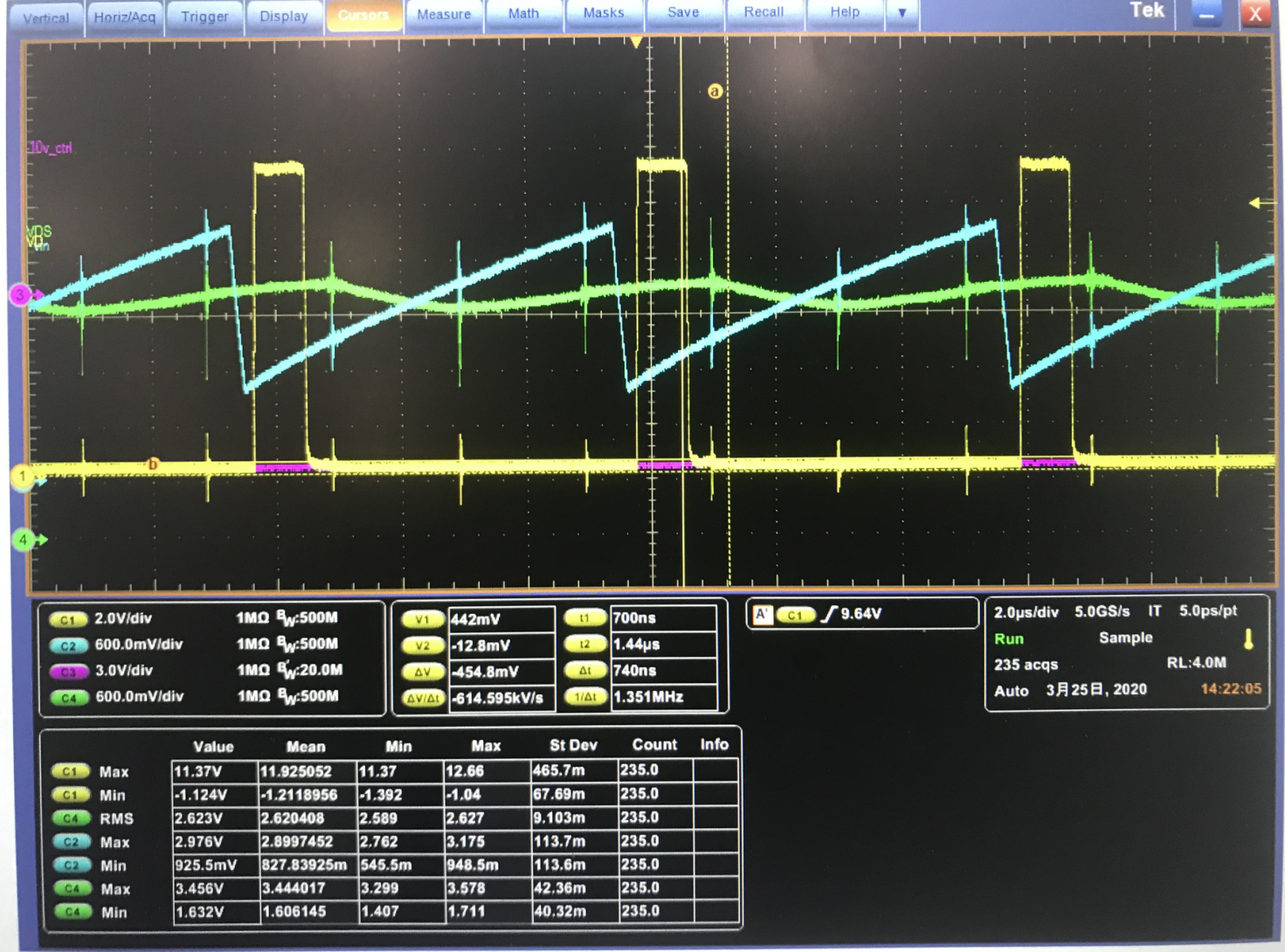
1. we found when Ton is large, there are two steps on OUT pin. Please kindly check the reason and if the 2rd step will drops lower.

Vin=34V Ch1=OUT, Ch2=RTCT, Ch4=Comp

Vin=55V, OUT pin signal is normal. Ton is smaller compared with above waveform
2. At same circuit, use AUX winding to power the Vcc pin. During power off, there is oscillation on Vcc. Please kindly check the reason.
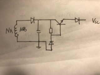
Ch4=Vcc

If change driver resistor from 100ohm to smaller value, such as 50ohm, there is no such oscillation.

BRs
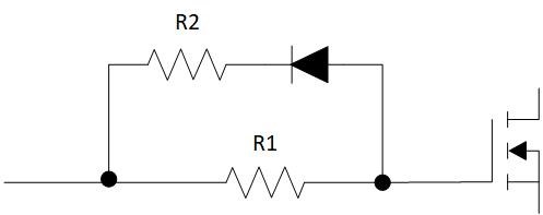
Given