This thread has been locked.

If you have a related question, please click the "Ask a related question" button in the top right corner. The newly created question will be automatically linked to this question.

LMG1210EVM-012: Genfet Q1 ( High Side getting blow of epc2001c )

Part Number: LMG1210EVM-012
Other Parts Discussed in Thread: LMG1210

Hi Support Team

We are using LMG1210EVM-012 evaluation board. 

Following are the input provide.

1. Providing +5V to LM1210 pin 4 via TP1 ( +5V DC ) and TP4 ( GND )

2. Providing +42V DC to via J2

3. Working in Independent Mode i.e J6 is shorted and J3 Open.

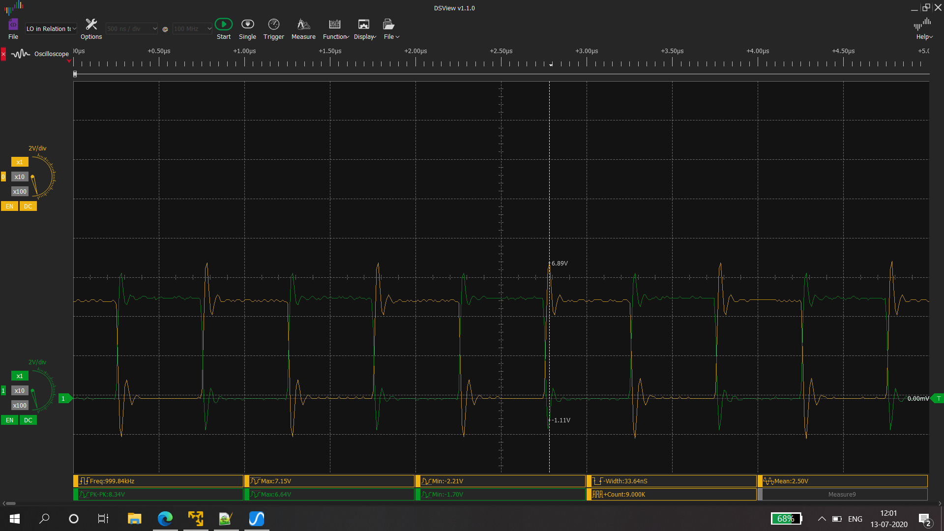
4. Providing a 100ns pulse of dead time of 10ns on PWM Low and PWM High . ( Please find the pdf attached for PWM_low and PWM high input )

5. Before testing we have simulated in TINA . Please find the attached tina circuit.

As we power on both +42V and +5V DC , both D2 and D2 is ON. Once we provide a PWM high and low pulse of 100ns . Q1 ( High Genfet ) is blowing OFF.

Kindly suggest on how to proceed further.

With Regards,

C P UmashankarTest Circuit 10ns dead time pulses at 50 50.TSCDead Time Explanation.pdf

  • Hi CP,

    Thanks for reaching out on e2e for lmg1210 EVM.

    Can you take a scope shot of HO with respect to HS on the same plot as LO with respect to VSS?

    That way we can see what the outputs are doing when the high-side FET burns.

    Also what is the HB-HS voltage during the time of failure?

    Thanks,

  • Hi Jeffrey Mueller,

    Thanks for the quick response.

    Can you take a scope shot of HO with respect to HS on the same plot as LO with respect to VSS?

    >> Attached png this capture is when We provide Vin ( LMG1210 ) = 12V DC to LMG1210 and Genfet with +5V DC

    That way we can see what the outputs are doing when the high-side FET burns.

    Also what is the HB-HS voltage during the time of failure?

    >> High Genfet is getting smoke unable to capture it. When we give We provide Vin ( LMG1210 ) = 12V DC to LMG1210 and Genfet with +42V DC

    Regards,

    C P U

  • Thanks CPU.

    Can you confirm that you are applying 12V  DC voltage to VIN?

    From the waveform the VIN voltage is pulsed and does not appear to be DC.

    Thanks,

  • Hi Jeffey Mueller,

    What we have used to LMG1210 is 12V DC only.

    Please see the Adapter used details.

    Regards,

    C P U

  • Thanks for the update CPU,

    Are you able to show a waveform of HB-HS voltage to determine if the high-side supply is getting charge to 5V during every switching cycle?

    Also, does the issue get better with a longer dead-time? or lower bus voltage?

    Thanks,

  • Hi Jefferry Muellur,

    Thanks for the responce.

    Are you able to show a waveform of HB-HS voltage to determine if the high-side supply is getting charge to 5V during every switching cycle?

    >> Yes we get high side is getting charged to 5v

    Also, does the issue get better with a longer dead-time? or lower bus voltage?

    >> Lower the deatime wave gets better. low voltage does not any impact.

    Today following are the experiment conduct

    Experiment 1 :


    ================================
    @ 12V Vin and 5V VDD 
    ================================

    HO High = 9.45 v
    Low = 85 mv

    LO High = 5.0 v
    Low = 85mv

    HS High = 5.0 v
    Low = 85 mv


    Experiment 2:

    ================================
    @ 12V Vin and 6V VDD 
    ================================

    HO High = 10.5 v
    Low = 85 mv

    LO High = 5.04 v
    Low = 85mv

    HS High = 6.04 v
    Low = 85 mv


    Experiment 3 :

    ================================
    @ 12V Vin and 9V VDD 
    ================================

    HO High = 13.5 v
    Low = 85 mv

    LO High = 5.04 v
    Low = 85mv

    HS High = 9.04 v
    Low = 85 mv


    Experiment 4:
    ================================
    @ 12V Vin and 12V VDD 
    ================================

    HO High = 16.5 v
    Low = 85 mv

    LO High = 5.04 v
    Low = 85mv

    HS High = 12.04 v
    Low = 85 mv


    Experiment 5 :
    ================================
    @ 12V Vin and 15V VDD temperature on High genfet shoots up to125c temperature
    ================================
    unable to measure

    Note :- Our requirement is to have a swing between 2.5V to 26.5 V on Vout line on J5. 

    Kindly provide your input on how to proceed further to achieve the same.

    Regards,

    C P U

  • HI CPU,

    Thanks for the update,

    When you say you apply 15V VDD, do you apply this voltage to J2 or TP1?

    also, VIN = 12V is being applied to J1?

    Are your inputs LI/HI and outputs LO/HO complementary to each other?

    is the dead-time set to 10ns or 100ns?

    do you have a load attached to the output when the high-side burns?

    Thanks,

  • Hi Jeffery Mueller,

    Thanks for the update,

    When you say you apply 15V VDD, do you apply this voltage to J2 or TP1?

    >> Apply Voltage on J2

    also, VIN = 12V is being applied to J1?

    >> Yes on J1

    Are your inputs LI/HI and outputs LO/HO complementary to each other?

    >> Now we are using PWM Mode ( 1us 50% duty cycle )

    is the dead-time set to 10ns or 100ns?

    >> Default 0.8 ns dead time.

    do you have a load attached to the output when the high-side burns?

    >> We did not had load connected. We will try with Load today and revert back to you.

    Kindly suggest any other changes we need to do.

    Regards,

    C P U

  • Hi CPU,

    Thanks for the update,

    With a 500ns pulse its possible that this pulse width is depleting the HB-HS bootstrap cap charge which is driving the high-side below saturation point and heating up the FET due to higher than normal Rdson.

    Can you replace the FET and confirm that the HB-HS voltage remains at 5V during all switching cycles?

    You can also try to increase the switching frequency to reduce the max pulse width at 50% duty cycle. This will allow a smaller pulse width to test with.

    Thanks,

  • Hi Jeffery Mueller,

    Thanks for the response. Based on your feedback after putting a capacitive load we were able to increase our High genfec Drain voltage upto 21V DC.

    With a 500ns pulse its possible that this pulse width is depleting the HB-HS bootstrap cap charge which is driving the high-side below saturation point and heating up the FET due to higher than normal Rdson.

    >> We now working with Independent mode , be feeding a 200ns period with duty cycle of 15% . Please find the pdf attached on how we are feeding en_hi and pwm low pin of LMG1210 input with ground in common between FPGA board and LMG1210 board ( picture  attached ).

    Can you replace the FET and confirm that the HB-HS voltage remains at 5V during all switching cycles?

    >> Yes we observer it is varying between 5.2 to 5.75 V .

    All the Above experiment is done by Feeding J1 ( VIN LMG1210 ) with 12VDC, J3 is short , J6 open, J2 ( VDD 21VDC) and load of 330uF capacitive ( 60 V rating capacitor ).

    Finally our actual load is 3.2uF and we should have swing in voltage between 2.5V to 26V . So kindly suggest on how to proceed further in achieving the same ?

    Attached the PWM high low pdf, setup picture and HO to HS Voltage png.

    Regards,

    C P U 200ns Hi Lo.pdf

  • Hi Jeffery Mueller,

    may be i missed attaching pwm wave form please find it attached to previous thread

    Regards,

    C P U2465.200ns Hi Lo.pdf

  • Hi CPU,

    Thanks for the update,

    Does the high side get burn?

    Or does the issue improve or dissapeared with your current test conditions?

    Thanks,

  • Hi Jeff,

    It is not burning but observation is temperature is shooting upto 130 degree Celsius. And difference between HO vs HS is around 5.7 v. As per datasheet if exceeds 6v it burn.

    We need an output swing vary between 27 v down to 2.5 v. As per present circuit we will not reach above 21v is it right ?

    All the Above experiment is done by Feeding J1 ( VIN LMG1210 ) with 12VDC, J3 is short , J6 open, J2 ( VDD 21VDC) and load of 330uF capacitive ( 60 V rating capacitor ).

    Finally our actual load is 3.2uF and we should have swing in voltage between 2.5V to 26V .

    So kindly suggest on how to proceed further in achieving the same ?

    Regards,

    C P U

  • Hi CPU,

    Thanks for the update,

    Seems to me this issue is thermal related. So if measures are taken to not create too much thermals on the evm it should not burn.

    Let me know if you have any other questions on this issue.

    Thanks,