This thread has been locked.

If you have a related question, please click the "Ask a related question" button in the top right corner. The newly created question will be automatically linked to this question.

TPS53681: Tps53681 + 6 * csd95490q5mc output current is imbalanced

Part Number: TPS53681
Other Parts Discussed in Thread: CSD95490Q5MC,

HI ,

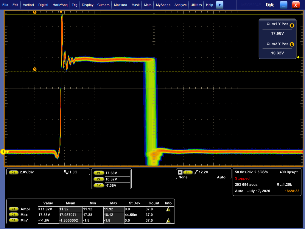
    Tps53681 + 6 * csd95490q5mc  output   current of phase-2  is imbalanced,

Excuse me, what causes current is unbalanced, and what aspects can I test to eliminate this problem.

  • Hi,

    Temperature is reporting as -70C. so Phase2 power stage is not switching. You can confirm this by measuring phase2 SW node waveform.

    Please check Phase2 powerstage VCC supply(5V) input.

    Thanks.

    Regards,

    Rama.

  • Hi,

    Please  update on this issue.

    Thanks.

    Regards,

    Rama.

  •    

    Hi,Rama. 

       Tps53681 + 6 * csd95490q5mc  output   current of phase-2  is imbalanced。This problem has been solved, the circuit has returned to normal, because we have a hardware problem

       I have another question,

     When our power supply is working, there will be a UVF alarm, and then turn off the power output.

    However, when we remove the resistance and capacitance from the SW, such as C41 and R51 in the figure below, this problem will not occur.

    Excuse me, what's the reason for this?

  • Hi,

    Thanks for update. Please provide details of hardware issue.

    on other question:

    • Are you seeing Vout UVF alarm during system running properly.i.e. Vout=0.755V? what is the boot voltage?
    • I don't have schematic of this project. Do you remove all phases snubber circuit or only one phase(C41 and R51)?
    • please confirm C41 is 1nF or 1uF?

    Thanks.

    Regards,

    Rama.

  • When there is a fault, there will be aVOUT  UVF alarm ,VOUT=0.755V  vboot is 0.755v  。 Other output voltage values will also have the same error phenomenon

    • I don't have schematic of this project. Do you remove all phases snubber circuit or only one phase(C41 and R51)?
      -------See attached schematic diagram,I deleted :R204/C1666  R205/C1667, R216/C1694,R217/C1695,R229/C1722,R228/C1723   The fault disappeared
    • please confirm C41 is 1nF or 1uF?
      ---------1nF

    4666.TPS53681+8x CSD95490Q5MC.pdf

  • Hi,

    so all phases snubber RC removed to work system properly.

    • we don't expect any issue with 1nF/1ohm snubber values. please check is there any wrongly connected 1uF cap instead of 1nF?
    • is system shutdown with UVF fault during boot-up conditions? or at steady-state after applying load?

    Thanks.

    Regards,

    Rama.

  • Hi, Rama.

    • we don't expect any issue with 1nF/1ohm snubber values. please check is there any wrongly connected 1uF cap instead of 1nF?

                ------------ I'm sure it's 1nF/0402 ,1ohm /0402 .  Does this resistor require power??   We use a 1 / 16 w 0402 package resistor

    • is system shutdown with UVF fault during boot-up conditions? or at steady-state after applying load?

                 ------------during boot-up conditions,There will be no UVF phenomenon and no power failure,After the load is working, UVF will appear,system will shutdown

    and ,Why is snuber RC not installed on datasheet and reference designs???as page 5 and page29 of ‘sluubp7’   page 107 of datasheet

    Thanks.

  • Hi,

    We will optimize power stage layout on TI web EVM. SW node ringing is less, so RC snubber is not required and it is DNP.

    We have tested EVMs with snubber connections also, don't see any issues like UVF..etc. This will reduce only SW node ringing.

    Typically suggested resistor package is 0603, but if we use 0402 size also, doesn't expected any fault/shutdown system.

    Thanks.

    Regards,

    Rama.

  • HI  ,

      Rama.

    “We will optimize power stage layout on TI web EVM. SW node ringing is less, so RC snubber is not required and it is DNP.”

    -------------You have optimized the layout. How did you optimize it? Do you have any relevant guidance documents?? Or what needs special attention

    “We have tested EVMs with snubber connections also, don't see any issues like UVF..etc. This will reduce only SW node ringing.”

    ------------What current and load change rate are you testing?

    and  Maybe we haven't found the real cause of the failure。

    We have removed the RC circuit. The equipment is working normally now, but the SW ringing amplitude will exceed the chip requirement (max 20V).

    If this parameter exceeds the chip requirement (max 20V), what fault will happen?

    thanks

  • Hi,

    • Yes. we do have layout guidelines to optimize layout. This document should be share under NDA restrictions. Do you have NDA with TI?, if yes, please mail to  ramasiddaiah@ti.com     do
    • Tested upto 50A/phase.
    • if SW node ringing is greater than 20V, we don't see any fault in system. At what load current are you seeing SW node ringing>20V?

    Thanks.

    Regards,

    Rama.

    • Yes. we do have layout guidelines to optimize layout. This document should be share under NDA restrictions. Do you have NDA with TI?, if yes, please mail to  ramasiddaiah@ti.com     do

             ----------We are in the process of signing DNA with Ti. When the contract is ready, I will send it to you

    • Tested upto 50A/phase.
      -------Have you tested the current dynamics?
    • if SW node ringing is greater than 20V, we don't see any fault in system. At what load current are you seeing SW node ringing>20V?

               -------When the RC circuit is removed,At 120A load current , SW node ringing about 21V,In case of higher current, we have no condition to test
    Attached is my PCB file, please see if there are any points that need to be optimized

    Is there any other reason that may cause this fault?


    1075840-SU8000-PCB166_0525_PCB.zip

  • Hi,

    Sure we will review layout. is TI team reviewed this layout earlier?. Provide TI FAE details for supporting this project.

    • Connect 1-phase RC snubber circuit and provide the below waveform during UVF fault shutdown. Please describe all test conditions also.

    Out put voltage waveform near to controller VSP/VSN waveform

    SW node waveform

    • SW node waveform at 120A load with differential probe(use GND point near to SW node)

    Initial review:

    i don't think, TI has reviewed this layout earlier as it is bad layout.

    • SW node should not have any vias and use only top side copper . but able to see more vias and top and bottom side copper.
    • Powerstage Vout sense feedback via and SW node snubber via is very near. so SW noise is coupling with Vout.
    • Powerstage VDD 2.2uF capacitor should be used bottom side powerstage GND, but here it is not correct and using faraway GND.
    • Bootstarp RC circuit should be placed same side of power stage(top side), but it is placed on bottom side.

    Thanks.

    Regards,

    Rama.

  • hi

    Rama.

         UVF fault shutdown, unable to test phase waveform.

    SW node waveform

    We found that the Vos pin is indeed coupled with the waveform of SW. If the RC circuit is removed, the coupling will be much smaller, so we suspect that the fault is caused here

    NDA mail has been sent to ramasiddaiah@ti.com Email, when can I get the layout guidance document???

    thanks

  • Hi,

    Thanks for update. I already replied yesterday as NDA has expired and need to renew this NDA.

    we are closing this ticket as replied to your mail.

    Regards,

    Rama.