This thread has been locked.

If you have a related question, please click the "Ask a related question" button in the top right corner. The newly created question will be automatically linked to this question.

UCC28180: Debug Steps

Part Number: UCC28180

Hi,

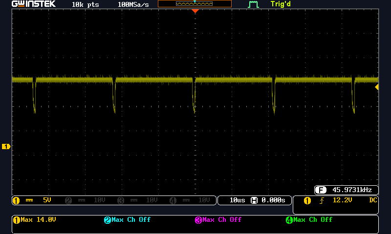
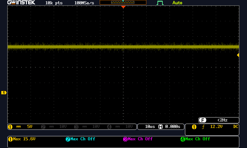
I have designed PFC stage according to TIDA-00779 using UCC27531D.

I have looking for a step by step debug process for UCC218180 like UCC28951, but I could not find. Do you have any resource to make circuit running step by step?

Is it possible to make some functionality test without AC Input? Like connecting a DC source to Vsense and Isense and adjust voltage levels simulating Input and Load to see gate signal.

Before connecting 230VAC to system I want to make sure everything is OK on controller side to prevetn a catastrophic failure.

Best Regards,

  • Hello Mert

    I'm afraid there isn't a debug process document for the UCC28180 - but here's a skeleton.

    Before putting any power on the input:

    Double check the connections from the device pins to their destinations.

    Apply 20V to Vout and measure the voltage at the VSENSE pin of the IC - it should be about 5% of Vref or about 250mV. This checks the output voltage sensing loop. At this time also check that the GND pin is at 0V -

    Remove the 20V from the output. Connect a variable source to VSENSE through a 1k resistor, set the source to 0V initially. Apply VCC (12V) to the controller.

    Measure the voltage at VCOMP - it should be high (>4V, but I'm not sure how high).

    Increase the voltage from the variable source until the VSENSE pin passes through 5V. As VSENSE reaches the 5V reference level the error amplifier should change state from HI to LO (close to 0V). This proves that the voltage regulation loop is working and with there earlier measurement you should expect the error amplifier to control the output at 400V.

    Check the frequency and amplitude of the GATE pulses at the MOSFET gate. Double check the ground connection from MOSFET source to GND of the controller.

    Check the connection from ISENSE to the current sense resistor. If you can, run 1A through the current sense resistor and verify that ISENSE is at a voltage of -1A*Rsense.

    Check the connection from the input, through the PFC inductor to the MOSFET drain and the diode Anode and then on to the bulk capacitor.

    Remove the gate drive resistor and tie the MOSFET gate to 0V through a 10k resistor (or a piece of wire)

    Apply a low DC voltage to the input (say 20V or so), the bulk capacitor should charge up to 20V (less a volt or so for the inptu bridge rectifier. Check the capacitor + is at 20V and the capacitor - is at 0V.

    Remove all the earlier connections. Set up a 'scope to monitor Vout, Vds and Vgs. Apply 20V to the input and the power stage should work. I'd run it only for as long as it takes to capture an image on the 'scope then turn it off immediately. (Don't forget to discharge the bulk capacitor with a resistor or an electronic load)

    If the waveforms look ok - then try again from AC.

    BTW: I'm working my way through your PCB layout - I hope to have something for you  this afternoon but I won't guarantee it.

    Regards

    Colin

  • Hi Colin,

    Thanks for the skeleton :)

    Colin: Double check the connections from the device pins to their destinations.

    Mert: Checked. It is OK

    Colin: Apply 20V to Vout and measure the voltage at the VSENSE pin of the IC - it should be about 5% of Vref or about 250mV. This checks the output voltage sensing loop. At this time also check that the GND pin is at 0V -

    Mert: Done. Vsense is 255mv. It is OK with calculations.

    Colin: Remove the 20V from the output. Connect a variable source to VSENSE through a 1k resistor, set the source to 0V initially. Apply VCC (12V) to the controller. 

    Measure the voltage at VCOMP - it should be high (>4V, but I'm not sure how high).

    Mert: Done. But It is 0.2V not >4V

    Colin: Increase the voltage from the variable source until the VSENSE pin passes through 5V. As VSENSE reaches the 5V reference level the error amplifier should change state from HI to LO (close to 0V). This proves that the voltage regulation loop is working and with there earlier measurement you should expect the error amplifier to control the output at 400V.

    Mert: Done. While increasing voltage when Vsense is 1.5V, Vcomp is 5V then when Vsense passes 5V Vcomp is going to low again (0.2V)

    Colin: Check the frequency and amplitude of the GATE pulses at the MOSFET gate. Double check the ground connection from MOSFET source to GND of the controller.

    Mert: Done. But I could not see the gate pulses, I see just high (Vcc of the driver) just increase Vsense to above 1.5V. Please find UCC28180 gate output scope below. As you can see frequency is OK but amplitude is not OK. Since it could not be 0V, gate drivers output is just only high.

    Since the last results are not correct, I stopped tests at this stage. Do you have any idea to what could cause to this problem?

    BTW: Thank you for your effort for checking layout, it is OK to get it tomorrow.

    Best Regards,

  • Hi Mert

    My mistake, COMP is held low by the FAULT switch (see the block diagram). The behaviour you saw while increasing the Vsense voltage is correct. VCOMP goes low when the VSENSE pin reaches the regulation reference voltage of 5V. I think this part of the circuit is ok.

    The OUT signal is running at Dmax and this does not allow enough time for the gate to discharge fully. Can you try again at the OUT test point TP1 ?

    I've emailed you the PCB review - you should have it now.

    Please let me know how you get on.

    Regards

    Colin

  • Hi Colin,

    Then Vcomp marked as OK. Thanks.

    The signal above was taken gate output of the controller. The scope of the TP1 is below.


    Thank you for your valuable review. I am appriciated.

    Best Regards.

  • Hi Mert

    I'm a bit confused here. The plot in your first post showed an active waveform running at 100kHz but the second shows only a DC level.

    The GATE output of the controller should be  rectangular wave, 0 to VDD amplitude running at maximum Duty cycle.

    The signal at the output of the driver should also be a rectangular wave -

    Can you re-check them.

    Regards

    Colin

  • Hi Colin,

    Yes it is confusing and nonsense. Therefore I have changed the conroller with a new one and everything is OK now.

    I have completed all the checks above everything is OK. I have applied AC and there is no problem except I could not get output above 336VDC.

    At around 100VAC output reaches 336VDC and never changes. Load is around 0.2Amps.

    I have checked Vsense it is around 4.3V 

    Below is the signal at gate.

    Do you have any suggestion for increasing output DC level?

    Best Regards,

  • Hello Mert

    The controller may be going into current limit so I'd suggest you double check the connections to the current sense resistor. The current sense resistor calculation is one of the steps in the Excel calculator for this product. Double check the sensing connections to this resistor - it's easy to pick up enough stray mOhms in the connections to significantly increase the effective value of this CS resistor. Run 1A from the bulk capacitor negative to the -ve terminal of the bridge rectifier and measure the voltage between the ISENSE and GND pins of the IC - does the measured resistance correspond with the nominal resistor value.

    Regards

    Colin